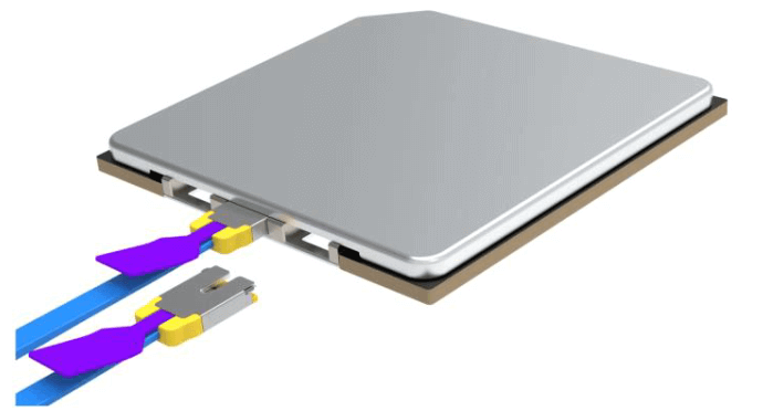
For CPO or Optical IO application scenarios, it is usually the first through the advanced package way to the optical chip and the electrical chip together, and then finally the optical fiber fixed to the optical chip. This will bring several problems. First of all, in the photoelectric chip before the completion of the package, it is not clear whether the performance of the chip meets the requirements, whether it is a good die or reduces the overall yield of the system. Secondly, after the optical fiber is glued to the optical chip, if there is a problem with the chip or the fiber coupling, it is more difficult to rework. In addition, the pigtail form of the optical fiber in the subsequent production process will bring the operation of the inconvenience, the user experience is also relatively poor. Therefore, Intel hopes to solve the above pain points, by developing a similar USB interface pluggable optical connector, that can be easily inserted into the CPO module, as shown in the figure below.
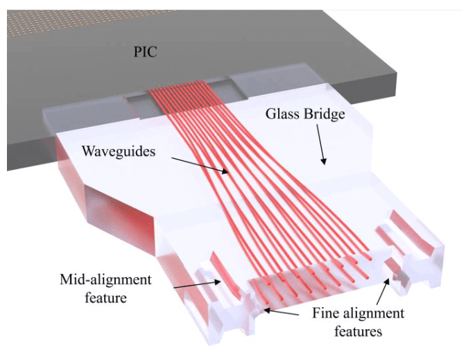
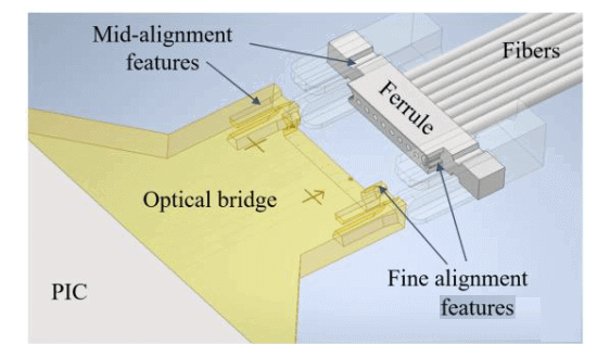
Intel proposed a glass optical bridge solution. Based on ultra-pulase laser direct writing, the ultra-short pulse of light will be focused to a specific depth in the glass chip, changing the optical properties of the local glass, and then processed 3-dimensional optical waveguide, its transmission loss of 0.2dB/cm. In addition, it can also be processed in the glass of the micro-mechanical structure, used for positional alignment. Intel’s glass optical bridge solution is shown in the figure below, where the glass containing the optical waveguide serves as an optical bridge to connect the silicon-based optical chip to an external optical connector. The 1*16 edge coupler output at the PIC in the figure can be converted to a 2×8 glass optical waveguide output through the 3D glass optical waveguide. Mechanical structures for alignment are also machined on this glass bridge, corresponding to the mid-alignment feature and fine-alignment feature in the figure below. The typical glass optical bridge has dimensions of 8.6mm*10mm*0.8mm.
The V-groove structure has been processed on the silicon optical chip, and the cylindrical bump structure has been processed on the glass bridge, which can be directly stuck into the V-groove by passive assembly, as shown in the figure below.
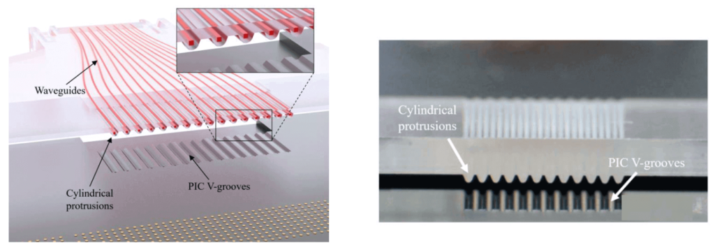
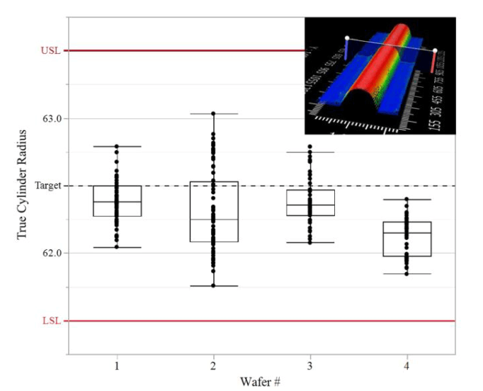
The role of the cylindrical protrusion is used to mimic the optical fiber, its design radius of 62.5um, the actual processing of the deviation of ± 0.084um (test samples for the 4-piece wafer, each wafer contains 48 pieces of die, each die on the 16-channel test structure), as shown in the figure below.
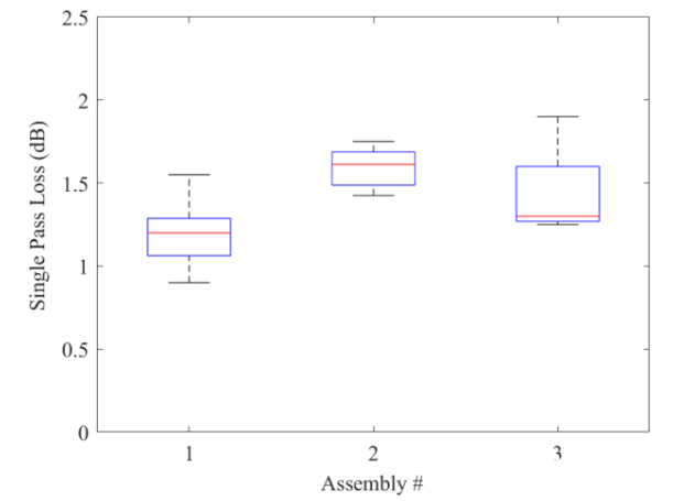
Further, Intel characterized the coupling loss of the PIC to the optical fiber through the glass bridging, and the average coupling loss for the three sets of structures was 1.19 dB, 1.59 dB, and 1.45 dB, respectively. The results of the tests are shown in the figure below, with an overall average coupling loss of 1.41 dB. The loss from the PIC to the optical bridging was 0.4 dB, and the loss from the optical fiber to the optical bridging was about 0.6 dB. Some additional loss is introduced due to processing errors in the mechanical structure.
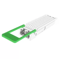
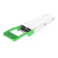
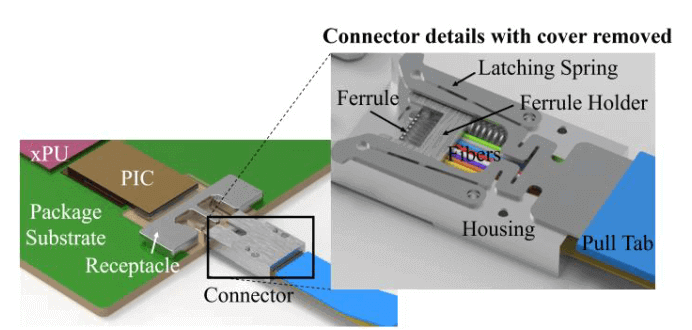
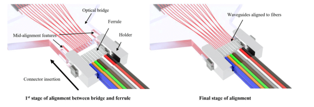
After the optical bridge and the PIC are assembled together, it is then necessary to develop a fiber-array unit connector (referred to as FAU) to connect with it, the structure of which is shown in the figure below. Fiber-array fixtures can be connected to the optical bridge through mechanical microstructures.
This FAU optical connector contains 5 main components: optical fiber clamps for fiber support and mechanical alignment, clamp bracket, latch spring, the entire connector shell, and socket on the optical bridge for pairing with the latch to fix it. The structural breakdown of the entire pluggable optical connector is shown in the figure below. In which the optical fiber clamp is also processed by laser direct writing, containing mechanical microstructures for alignment and holes for fiber alignment, the tolerance of the fiber alignment holes is ± 0.5um.
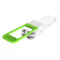
During connector use, the ferrule holder is first inserted into the coarse alignment structure on the optical bridge, and further, the mechanical microstructure is utilized to achieve fine alignment, the whole pairing process is shown in the figure below. A spacing of about 10um is retained between the final optical bridge and the FAU connector, and both interfaces are designed to be slanted at 8 degrees to minimize back reflection.
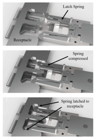
The latching spring is designed to ensure an effective and tight connection between the optical connector and the glass bridge. When the connector is inserted into the optical bridge, the spring is pushed inward by extrusion. When the latch is successfully matched with the receptacle, the spring will be released externally to ensure that the two are effectively attached, as shown in the following figure.
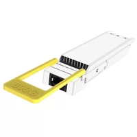
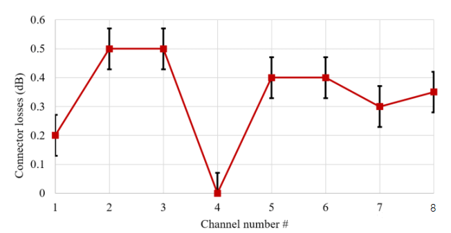
The average optical loss of the connector is 0.33dB, and the test results are shown below.
To summarize, Intel has processed three-dimensional optical waveguides and mechanical microstructure in glass by laser direct writing technology to form a glass optical bridge to connect with a silicon optical chip. As for the pluggable optical connector, the laser writing technology is also used to process the optical fiber clamp and mechanical microstructure. The mechanical microstructures on the optical connector and optical bridge are aligned and paired to realize the function of a pluggable optical connector. The whole solution design is very ingenious. The optical loss of the single end of the solution is 1.41dB (optical connector->optical bridge->silicon optical chip), while the optical loss of the connector is 0.33dB (optical connector->optical bridge), which is better than the general performance of the edge coupler index. With this pluggable optical connector, the silicon optical chip can be tested first, and the good die can be screened for packaging, which reduces the packaging cost, can greatly improve the yield of the CPO module, and solves a difficult problem of CPO/Optical IO technology landing.
Related Products:
-
 OSFP-800G-FR4 800G OSFP FR4 (200G per line) PAM4 CWDM Duplex LC 2km SMF Optical Transceiver Module
$3500.00
OSFP-800G-FR4 800G OSFP FR4 (200G per line) PAM4 CWDM Duplex LC 2km SMF Optical Transceiver Module
$3500.00
-
QSFP-DD-800G-2FR2L 800G QSFP-DD800 2FR2 (200G per line) 2km 1291/1311nm Dual Duplex LC SMF Transceivers
$3000.00
-
OSFP-800G-DR4 800G OSFP DR4 (200G per line) PAM4 1311nm MPO-12 500m SMF DDM Optical Transceiver Module
$3000.00
-
QSFP-DD-800G-FR4 800G QSFP-DD800 FR4 (200G per line) PAM4 CWDM 2km DOM Duplex LC SMF Optical Transceiver Module
$3500.00
-
OSFP-800G-SR8D-FLT OSFP 8x100G SR8 Flat Top PAM4 850nm 100m DOM Dual MPO-12 MMF Optical Transceiver Module
$650.00
-
OSFP-800G-FR8L OSFP 800G FR8 PAM4 CWDM8 Duplex LC 2km SMF Optical Transceiver Module
$3000.00
-
QSFP-DD-800G-FR8L QSFP-DD 800G FR8 PAM4 CWDM8 2km DOM Duplex LC SMF Optical Transceiver Module
$3000.00
-
QSFP-DD-800G-LR8D QSFP-DD 8x100G LR PAM4 1310nm 10km Dual MPO-12 SMF FEC Optical Transceiver Module
$1550.00
-
QSFP-DD-800G-LR8 QSFP-DD 8x100G LR PAM4 1310nm 10km MPO-16 SMF FEC Optical Transceiver Module
$1600.00
-
OSFP-800G-2FR4L OSFP 2x400G FR4 PAM4 1310nm 2km DOM Dual Duplex LC SMF Optical Transceiver Module
$1200.00