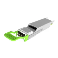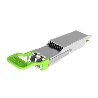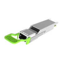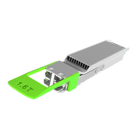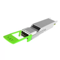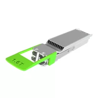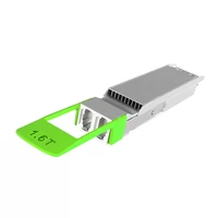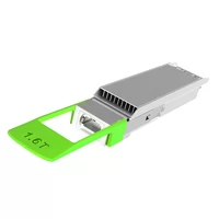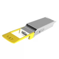

USFP (Ultra-Dense Small Form Factor Pluggable) is the new optical transceiver form factor from NVIDIA and Cisco that brings 400 Gb/s-per-lane electrical signaling to AI factory networking. Announced at OCP Global Summit 2026, it packs 16 full-duplex lanes into an OSFP-sized footprint, roughly 6.4 Tb/s per module, with a published path to 12.8 Tb/s.
Here’s the blunt version: AI clusters are putting increasing pressure on today’s pluggable optics. Every large deployment needs more GPUs, more bandwidth, and tightly controlled latency. The 200 Gb/s-per-lane SerDes used in many current 800G and 1.6T designs can make it harder to increase port density without adding more switch capacity, optical links, or network tiers. A 400G/lane design could help address that challenge, although the actual benefit will depend on the host platform and network architecture.
What Is USFP?
USFP stands for Ultra-Dense Small Form Factor Pluggable. It is a high-density optical transceiver form factor announced by NVIDIA and Cisco at OCP Global Summit 2026. The companies plan to develop an open industry specification through a community-led multi-source agreement (MSA). The design targets 400 Gb/s-per-lane electrical signaling, but the announcement should not be treated as a finalized specification.
The name reflects its high-density design goal. Current dense pluggable formats such as OSFP and QSFP-DD support electrical lanes of up to 200 Gb/s in their latest configurations. USFP is designed to double the per-lane rate to 400 Gb/s, potentially delivering more aggregate bandwidth within a similar front-panel footprint. That can improve bandwidth density, but it does not automatically mean fewer switches, fewer network tiers, or a lower cost per gigabit; those outcomes depend on switch silicon, port configuration, topology, and system power requirements.
For a deeper comparison of the form factors themselves, see our USFP vs OSFP vs QSFP-DD comparison. Here, we focus on what USFP could mean for AI factory networks.
Why AI Factories Are Outgrowing Today’s Optics
AI factories are not ordinary data centers. The term describes facilities built to produce AI tokens at scale, running large training and inference workloads across thousands of accelerators. Their network requirements are demanding across three dimensions: bandwidth, latency, and density.
The 200G/Lane Ceiling
Optical module capacities have climbed steadily from 40G and 100G to 400G, 800G, and 1.6T. On the electrical side, the SerDes lane rate that feeds the optics has also advanced, but many current 800G and 1.6T designs still use 100G or 200G-per-lane signaling. At 200G per lane, a 1.6T interface requires eight lanes, while a 3.2T interface would require 16. Higher lane counts can increase pressure on connector design, signal integrity, power delivery, and thermal management.
USFP is designed to address this scaling challenge by supporting 400G-per-lane electrical signaling. At a given aggregate capacity, doubling the lane rate can reduce the number of electrical lanes required. The resulting density and power benefits, however, depend on the host ASIC, module implementation, and system design.
Front-Panel Density and Power Limits
Market forecasts underline the pace of the transition. In May 2025, Cignal AI forecast that 800G datacom optics would be the fastest-growing segment and that shipments would grow by about 60% in 2025. Later market reporting put the estimate for 2025 shipments of high-speed modules at 800GbE and above at roughly 42 million units, while 1.6T adoption continued to ramp. Cignal AI market materials have also projected that blended high-speed datacom module costs could approach $0.50 per Gbps by 2027. These figures are market estimates or forecasts, not USFP-specific projections, and they can change as deployment plans evolve.
NVIDIA and Cisco say USFP is designed to deliver roughly four times the front-panel bandwidth density and about 1.3 times the power efficiency of 200G-per-lane pluggable optics. These are vendor-stated design targets rather than independently verified results from commercially deployed USFP modules. If achieved in a given system, they could help operators manage rack space, network capacity, and power budgets.
USFP Technical Specifications
USFP is at the announcement and ecosystem-development stage. The following points describe the design targets disclosed by NVIDIA and Cisco, rather than a finalized, independently ratified specification.
400G/Lane Electrical Signaling
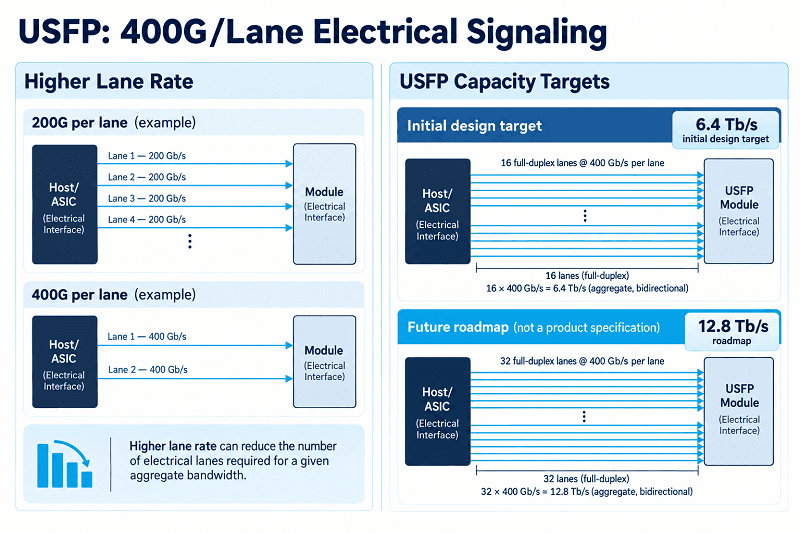
USFP is designed to support 400 Gb/s-per-lane electrical signaling. This doubles the lane rate used in many current high-density pluggable designs and could provide a path to greater bandwidth density. The electrical lane rate should not be confused with the optical wavelength count or the data rate of an individual optical channel; the actual optical implementation will depend on the module design.
16 Lanes to 6.4T, Scaling to 12.8T
The first planned USFP-based transceivers are expected to pack 16 full-duplex lanes into an OSFP-sized footprint. At 400 Gb/s per lane, this corresponds to 6.4 Tb/s of aggregate capacity. The design is intended to scale to 32 full-duplex lanes, creating a path to 12.8 Tb/s. This roadmap could support future high-capacity AI fabrics, but realized capacity and port mapping will depend on the host system and final implementation.
The 2D-Array Connector and 100W Thermal Envelope
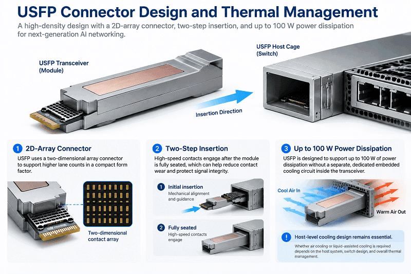
Rather than simply extending the single-row edge connector used by established pluggable formats, USFP uses a new two-dimensional array connector with a two-step insertion design. According to the announcement, high-speed contacts engage after the module is inserted, a design intended to reduce contact wear, improve signal integrity, and make insertion force more predictable.
USFP is designed to support power dissipation of up to 100 W without a separate, dedicated embedded cooling circuit inside the transceiver. This may simplify module design, but it does not eliminate the need for adequate cooling at the host-system level. Whether a deployment can use air cooling or requires liquid-assisted cooling will depend on the switch, cage, heatsink, airflow, and overall thermal design. The 800 V DC power-distribution trend is a separate consideration from rack power density; voltage and power density should not be used interchangeably.
USFP vs OSFP vs QSFP-DD vs XPO vs CPO
USFP is one of several approaches being explored for higher-capacity AI networking. Each makes a different trade-off between lane rate, lane count, serviceability, cooling, and integration. The figures below summarize published specifications or announced design targets; they should not be read as a like-for-like comparison of commercially available products.
| Form Factor | Width / Footprint | Electrical Lanes | Per-Lane Speed | Aggregate Capacity | Cooling | Status |
| QSFP-DD | Approx. 18.4 mm wide | 8 | Up to 200G | Up to 1.6T (QSFP-DD1600) | Depends on module and host; enhanced cooling may be needed | Established MSA; products shipping |
| OSFP | Approx. 22.6 mm wide | 8 | Up to 200G | Up to 1.6T | Integrated heatsink in standard OSFP designs | Established MSA; products shipping |
| USFP | OSFP-sized target | 16 initially; roadmap to 32 | 400G target | 6.4T initially; roadmap to 12.8T | Up to 100 W dissipation; host cooling dependent | Announced design; MSA planned |
| OSFP-XD | Distinct OSFP-XD form factor | 16 | Up to 200G | Up to 3.2T | Depends on module and host design | Published MSA specification; implementation dependent |
| XPO (Arista) | Larger, design-specific | 64 in the published concept | 200G target | Up to 12.8T target | Liquid cold plate in the published concept; power is design-specific | Roadmap / proposed architecture |
| CPO | On-package or near-package; not a front-panel pluggable | Varies | Varies | Varies | System-dependent; liquid cooling may be used | Emerging, implementation-specific |
The main distinction is that USFP emphasizes faster electrical lanes, targeting 400G per lane. XPO emphasizes a larger number of lanes, with a published concept based on 64 lanes at 200G per lane. CPO moves optical engines closer to the switch ASIC, changing the balance between integration, thermal design, and serviceability. OSFP-XD is another high-density pluggable option: its MSA specification supports 16 electrical lanes and up to 3.2 Tb/s at 200G per lane. OSFP-XD is mechanically and electrically distinct from standard OSFP and is not interchangeable with it.
There is no universal winner. USFP aims to retain the familiar pluggable, field-serviceable model while increasing bandwidth density. OSFP-XD offers a specified 3.2T path using 200G lanes, while XPO and CPO explore different approaches to higher capacity and integration. The best fit will depend on qualified host platforms, power and cooling constraints, ecosystem support, and deployment requirements.
How USFP Changes AI Factory Network Architecture
The form factor is only part of the story. The architectural impact depends on where the modules are deployed and how the switch fabric is designed.
Backend vs Frontend, and Scale-Up vs Scale-Out
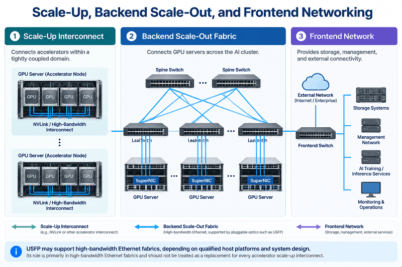
AI factory networks are often described in terms of backend and frontend networks, as well as scale-up and scale-out domains. These terms are related, but they are not interchangeable. A scale-up interconnect connects accelerators within a tightly coupled domain, while a scale-out fabric connects servers or accelerator systems across a larger cluster. A backend fabric commonly carries high-performance traffic among AI servers; frontend networking may connect the cluster to storage, management systems, enterprise services, and external networks. The exact division varies by architecture.
The planned USFP transceivers are intended for use in switches and SuperNICs, making them relevant to high-bandwidth Ethernet fabrics. They should not automatically be treated as a replacement for every short-reach scale-up interconnect, such as a dedicated GPU interconnect. Their role will depend on the host platform, optical implementation, and network design. NVIDIA and Cisco say USFP could help operators connect more 1.6T endpoints without adding network tiers, but that outcome is not guaranteed for every deployment.
Rail-Optimized Designs and SuperNICs
Modern AI clusters often use rail-optimized topologies, distributing GPU traffic across multiple network paths or switches to help manage congestion and maintain predictable performance. These designs are sensitive to port density, link count, oversubscription, and cabling. At a fixed aggregate capacity, 400G electrical lanes can reduce the number of electrical lanes needed compared with 200G lanes. Whether that also reduces external optical links, cables, or switch count depends on the port and breakout configuration.
Connecting More 1.6T Endpoints Without Added Tiers
Higher-capacity pluggables could give switch designers more options for connecting 1.6T endpoints and building higher-radix fabrics. NVIDIA and Cisco position USFP as a way to increase capacity without necessarily adding network tiers. In practice, the result will depend on the switch ASIC’s total bandwidth and radix, the number and type of ports, the network topology, and the chosen oversubscription ratio. Fewer tiers can reduce hop count and latency in some designs, but those benefits must be demonstrated at the system level rather than assumed from the module form factor alone.
Migration Path: From 200G/Lane to 400G/Lane
Operators are unlikely to replace a working fabric overnight. The practical question is how a network built around 200G-per-lane components could evolve as 400G-per-lane systems become available.
Compatibility with Existing OSFP/QSFP-DD Estates
USFP is a new form factor, not a drop-in replacement for OSFP or QSFP-DD. Existing 800G and 1.6T modules will continue to operate in their qualified cages and ports. USFP deployment will require compatible USFP cages, connectors, modules, and host platforms. If and when compatible 400G-per-lane switch silicon and systems become commercially available, operators could introduce USFP-based ports alongside existing infrastructure rather than replacing the entire network at once.
Spectrum-X and Silicon One Interoperability
The USFP initiative builds on NVIDIA and Cisco’s existing work to enable interoperability between NVIDIA Spectrum-X Ethernet networking and Cisco Silicon One-based Ethernet platforms. That collaboration supports the goal of a shared, cross-vendor ecosystem. However, existing platform interoperability does not mean that every future USFP module or host configuration has already been validated. Cross-vendor USFP interoperability will depend on the finalized specification, qualified products, and system-level testing.
The Road to Commercial Reality
The key point is that USFP is currently an announced design initiative, not a generally available product.
MSA Status, Ecosystem Partners, and Missing Silicon
NVIDIA and Cisco are working with TE Connectivity and Amphenol on USFP cages, connectors, and modules, with additional partners expected to join. They plan to create an open industry specification through an upcoming community-led multi-source agreement (MSA). The public announcement did not specify a sampling schedule or commercial availability date. Broad deployment will also depend on compatible host silicon, finished modules, system qualification, and interoperability testing. Until those pieces are available, USFP should be treated as a roadmap rather than a product that operators can deploy today.
Competing Bets: XPO, OSFP-XD, CPO
USFP is not guaranteed to become the dominant standard. Arista’s XPO explores a higher-lane-count approach, OSFP-XD provides a published path to 3.2T using 200G electrical lanes, and CPO moves optics closer to the switch package. Each approach has different implications for bandwidth density, cooling, manufacturing, field replacement, and supply-chain flexibility. Network operators should compare qualified system-level implementations rather than choosing based on a form factor’s headline capacity alone.
Conclusion
USFP is an important signal that the industry is preparing for optical networking beyond 200G-per-lane electrical signaling. Announced by NVIDIA and Cisco, the planned form factor targets 400G-per-lane signaling, 16 full-duplex lanes, and 6.4 Tb/s of initial aggregate capacity, with a roadmap to 12.8 Tb/s. The companies say the design aims to deliver roughly four times the front-panel bandwidth density and 1.3 times the power efficiency of 200G-per-lane pluggable optics. Those figures remain vendor-stated design targets, and the final specification, host compatibility, product availability, and real-world benefits will need to be validated as the ecosystem develops.
Related Products:
-
 OSFP-XD-1.6T-4FR2 1.6T OSFP-XD 4xFR2 PAM4 1291/1311nm 2km SN SMF Optical Transceiver Module
$5000.00
-
OSFP-XD-1.6T-2FR4 1.6T OSFP-XD 2xFR4 PAM4 2x CWDM4 2km Dual Duplex LC SMF Optical Transceiver Module
$5000.00
-
OSFP-XD-1.6T-DR8 1.6T OSFP-XD DR8 PAM4 1311nm 2km MPO-16 SMF Optical Transceiver Module
$4500.00
-
NVIDIA MMS4A00 (980-9IAH1-00XM00) Compatible 1.6T 2 x DR4/DR8 OSFP224 PAM4 1311nm 500m IHS/Finned Top Dual MPO-12 SMF Optical Transceiver Module
$1500.00
-
NVIDIA MMS4A50 Compatible 1.6T 2xFR4/FR8 OSFP224 PAM4 1310nm 2km IHS/Finned Top Dual Duplex LC SMF Optical Transceiver Module
$1800.00
-
NVIDIA MMS4A00-RHS Compatible 1.6T 2xDR4/DR8 OSFP224 PAM4 1311nm 500m RHS/Flat Top Dual MPO-12/APC InfiniBand XDR SMF Optical Transceiver Module
$2000.00
-
OSFP-1.6T-4FR2 1.6T OSFP 4FR2 PAM4 1291/1311nm 2km SN SMF Optical Transceiver Module
$3500.00
-
OSFP-1.6T-2FR4 1.6T OSFP 2xFR4 PAM4 2x CWDM4 2km Dual Duplex LC SMF Optical Transceiver Module
$1800.00
-
OSFP-1.6T-DR8D+ 1.6T OSFP DR8D+ PAM4 1311nm 2km Dual MPO-12 SMF Optical Transceiver Module
$3500.00
-
OSFP-1.6T-DR8+ 1.6T OSFP DR8+ PAM4 1311nm 2km MPO-16 SMF Optical Transceiver Module
$3000.00
-
OSFP-1.6T-DR8D 1.6T 2 x DR4/DR8 OSFP224 PAM4 1311nm 500m Dual MPO-12 SMF Optical Transceiver Module
$1500.00
-
OSFP-1.6T-DR8 1.6T 2 x DR4/DR8 OSFP224 PAM4 1311nm 500m MPO-16 SMF Optical Transceiver Module
$3000.00