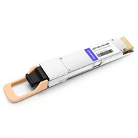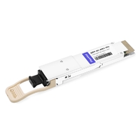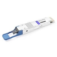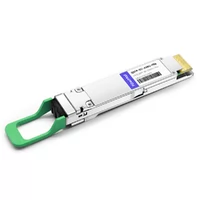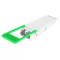

400G per lane refers to a nominal data rate of 400 gigabits per second (Gb/s) carried by a single electrical lane or optical data channel, depending on the interface being discussed. It represents the next step beyond the 200G-per-lane signaling used in 1.6T-class modules. For electrical interfaces, the industry often discusses a 448 Gb/s gross signaling rate. If PAM4 is used, this corresponds to approximately 224 GBaud. However, the final modulation and coding choices for 448G interfaces are still under development. This technology could help scale optical modules from 1.6T to 3.2T and eventually to 6.4T and beyond.
Here’s why the number matters. Optical module capacity is generally calculated by multiplying the number of lanes by the data rate per lane. A 1.6T OSFP module, for example, can use eight host-side electrical lanes operating at 200G each. A future 3.2T architecture could use the same number of electrical lanes at 400G each. This would double aggregate bandwidth without increasing the electrical lane count. However, it would not necessarily keep the same fiber count: that depends on the optical interface and how its channels are implemented.
What “Per Lane” Actually Means in an Optical Transceiver
Every optical module is, at heart, a multiplication problem. The aggregate bandwidth of an interface is the number of lanes multiplied by the data rate of each lane. This is a useful way to understand the evolution of optical networking, but a transceiver has separate host-side electrical and line-side optical interfaces, and their lane counts do not always match.
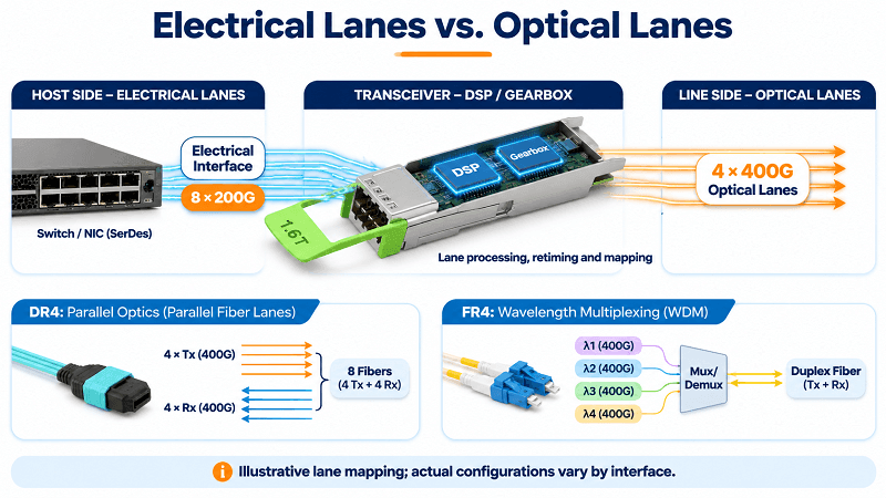
Take a 400G QSFP-DD module. Early 400G QSFP-DD implementations commonly used eight electrical lanes at 50G each, for 8 × 50G = 400G. A 400G DR4 optical interface, by comparison, uses four optical lanes at 100G each, for 4 × 100G = 400G. The aggregate capacity is the same, but the lane architectures are different and refer to different sides of the transceiver.
This is why “per lane” matters more than the headline number. The lane rate strongly influences signaling complexity, signal-integrity requirements, and which switch silicon can drive the interface. Power consumption also depends on the DSP architecture, optical components, reach, and cooling design. The number of fibers required depends on the line-side architecture, including whether it uses parallel optical lanes or wavelength-division multiplexing (WDM). When an engineer asks about “400G per lane,” they are usually asking about the performance requirements of a specific electrical or optical interface, not just the module’s aggregate capacity.
The lane-rate progression is the clearest way to anchor the term.
| Lane rate | Modulation | Illustrative example | Approximate era |
| 25G | NRZ | 100G QSFP28 (4 × 25G electrical lanes) | 2010s |
| 50G | PAM4 | 400G QSFP-DD (8 × 50G electrical lanes); 200G QSFP56 (4 × 50G electrical lanes) | 2018+ |
| 100G | PAM4 | 800G QSFP-DD/OSFP (8 × 100G electrical lanes); 400G DR4 (4 × 100G optical lanes) | 2020s |
| 200G | PAM4 | 1.6T OSFP (8 × 200G electrical lanes) | 2026+ |
| 400G | PAM4, PAM6, or PAM8 under evaluation | Potential 3.2T architecture (8 × 400G electrical lanes) | Emerging; 2027–2029 outlook |
For the full picture on how the 1.6T and 3.2T rungs of that ladder are built, FiberMall’s 1.6T and 3.2T optical transceiver guide walks through the architecture in detail.
Electrical Lanes vs. Optical Lanes: Where the Term Splits
Here is the single most common source of confusion, and it is worth a section of its own. “400G per lane” can refer to different interfaces on the two sides of a transceiver.
The Host Side: Electrical Lanes
On the host side, the transceiver connects to a switch or NIC. The “lanes” are electrical SerDes signals carried through the host PCB, connector, and module interface. In discussions of 400G-per-lane electrical interfaces, a 448 Gb/s gross signaling rate is often used as the reference point. If PAM4 is selected, 448 Gb/s corresponds to approximately 224 GBaud because each PAM4 symbol carries two bits.
It is important not to interpret 448 Gb/s as a universal formula for 400 Gb/s of payload plus a fixed amount of FEC overhead. The relationship between nominal data rate, gross signaling rate, coding, and FEC depends on the interface specification and implementation. This is one of the hardest parts of the system because the electrical channel must cope with insertion loss, crosstalk, connector limitations, and tight bandwidth constraints.
The Line Side: Optical Lanes
On the line side, optical lanes are independent optical data channels transmitted over fiber. Depending on the optical architecture, they may be implemented as parallel fiber lanes, as in DR4, or as wavelength-multiplexed channels, as in FR4.
An optical channel carrying 400G may be described as a 400G optical lane. The more specific term “400G per lambda” means that a single optical wavelength carries 400 Gb/s. The two terms are related, but they are not interchangeable in every architecture: an optical lane does not always correspond to a separate wavelength. The modulation and detection method also depend on the application; IMDD is common in data-center optics, while coherent technology is used in other optical systems.
The bridge between the two sides may include a DSP with an integrated gearbox function. A gearbox changes the number or rate of lanes between interfaces, while the DSP can also perform functions such as equalization and signal recovery. For example, a module architecture could map eight 200G electrical lanes on the host side to four 400G optical channels on the line side. This is an illustrative architecture, not a requirement for every transceiver.
The Lane-Rate Roadmap: From 25G NRZ to 400G PAM4
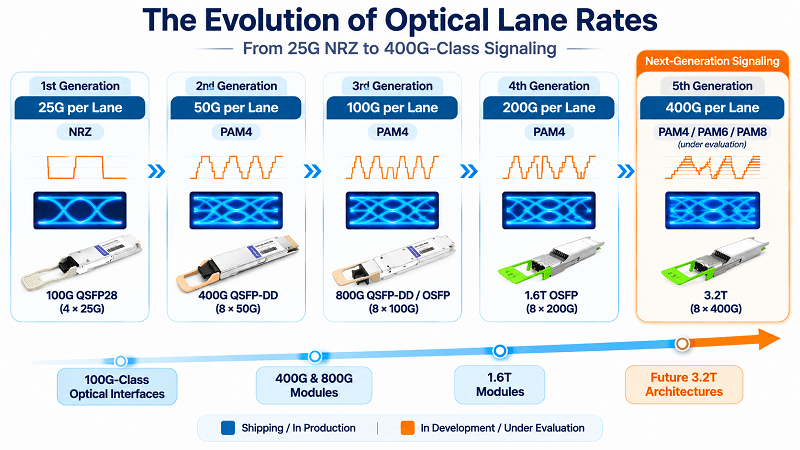
The lane-rate progression is one of the clearest trends in optical networking. It has often advanced in doubling steps, with each major increase driving changes in signaling technology, electrical interfaces, and module design. However, a higher lane rate does not automatically dictate one specific modulation scheme or form factor.
NRZ and the 25G Era
Early generations of high-speed data-center modules used NRZ, or non-return-to-zero, which encodes one bit per symbol using two signal levels. A 100G QSFP28 module used four lanes of 25G NRZ. The technology was relatively simple and power-efficient, with signal-integrity requirements that were manageable for the interfaces of that generation. It therefore became widely used in data-center optics through the 2010s.
PAM4 and the 50G/100G Lanes
The move to 400G aggregate capacity accelerated the adoption of PAM4, which encodes two bits per symbol using four signal levels. This allowed 400G modules to use eight electrical lanes of 50G PAM4. Later, optical interfaces such as DR4 and FR4 used four 100G optical channels to deliver 400G aggregate bandwidth. The host-side electrical lane mapping can vary by module and host interface.
200G per Lane: Today’s State of the Art
200G per lane is the current high-end generation for pluggable data-center optics. A 1.6T OSFP module can use eight electrical lanes of 200G PAM4. Depending on the specific interface and implementation, the symbol rate is approximately 106–112 GBaud. This generation provides the baseline against which 400G-per-lane technologies are being developed.
400G per Lane: The Next Generation
400G per lane doubles the nominal lane data rate again. One candidate electrical implementation uses 448 Gb/s gross PAM4 signaling at approximately 224 GBaud. However, PAM4 is not yet a settled choice for all 400G-per-lane interfaces: PAM6 and PAM8 are also being evaluated because they can reduce the required symbol rate, although they impose tighter signal-to-noise requirements.
The capacity calculation is straightforward: eight electrical lanes operating at 400G each would deliver 3.2T of aggregate bandwidth. A 3.2T platform could then provide a stepping stone to 6.4T and higher-capacity architectures. The challenge is that 400G-per-lane signaling places much greater demands on SerDes silicon, connectors, packages, PCB materials, and signal processing. The final implementation will depend on standards development and system-level trade-offs.
PAM4 vs NRZ: Why Faster Lanes Need New Modulation
As lane rates increase, NRZ becomes increasingly difficult to use because it requires a higher symbol rate to carry the same amount of data. NRZ encodes one bit per symbol with two signal levels. PAM4 encodes two bits per symbol with four levels, so it can carry twice as much data at the same baud rate.
The trade-off is noise tolerance. With the same overall signal swing, the spacing between adjacent PAM4 levels is approximately one-third of the NRZ eye opening. This smaller separation makes PAM4 more sensitive to noise, distortion, and jitter. High-speed PAM4 links commonly use FEC and signal equalization to maintain link performance, but the need for an in-module DSP depends on the transceiver architecture. Linear-drive solutions, for example, can reduce or eliminate the need for a conventional module DSP.
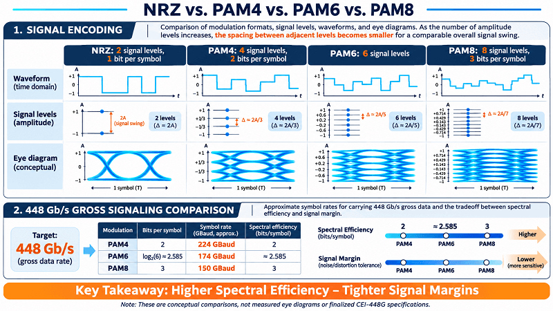
This challenge becomes more pronounced at 448 Gb/s gross signaling. A 224-GBaud PAM4 signal has a Nyquist frequency of approximately 112 GHz. OIF’s Next Generation CEI-448G Framework discusses the limitations of existing package and connector channels, some of which are around 90 GHz, and examines higher-order modulation such as PAM6 and PAM8 as possible alternatives. These formats reduce the required symbol rate to approximately 174 GBaud and 150 GBaud, respectively, but the smaller spacing between signal levels increases SNR requirements. The framework discusses possible approaches; it does not establish a final modulation choice for CEI-448G.
The practical takeaway for a network engineer is that faster lanes require more advanced channel design, signal equalization, and often stronger error-correction capabilities. The exact DSP architecture and modulation format will depend on the interface and system design.
The Standards Behind 400G per Lane
400G per lane is not a single vendor’s invention. Work is progressing through industry standards organizations, and understanding the status of these projects helps clarify the technology’s development timeline.
OIF CEI-448G: The Electrical Interface
The Optical Internetworking Forum (OIF) published its Next Generation CEI-448G Framework on November 4, 2025. The framework identifies application spaces, technical challenges, and potential solution paths for 448G-per-lane electrical interfaces. It is an informative framework document, not a finalized implementation agreement.
In February 2026, OIF initiated the CEI-448G-VSR chip-to-module project and the CEI-448G-LR backplane project, building on earlier CEI-56G, CEI-112G, and CEI-224G work. The OIF project announcement outlines the scope of the new work. The modulation format and detailed interface requirements remain under development.
IEEE 802.3dv: The Ethernet Standard
In parallel, the IEEE 802.3 Working Group chartered a 400 Gb/s-per-lane Signaling Study Group in March 2026. The Project Authorization Request (PAR) for IEEE P802.3dv was approved on September 25, 2026, and the work has moved into the Task Force stage. The project aims to develop Ethernet physical-layer specifications and management parameters for 400 Gb/s, 800 Gb/s, and 1.6 Tb/s interfaces using 400 Gb/s-per-lane signaling over electrical interconnects and single-mode fiber optical links with reaches of up to 500 meters. The current status is available on the IEEE P802.3dv project page.
The sequencing is the useful signal. Frameworks and approved project scopes establish the direction, but they do not mean the final specifications are complete. The next steps include selecting technical proposals, completing the specifications, developing compatible silicon, and validating modules. That is the gap between “400G per lane is coming” and “400G-per-lane modules are widely available.”
The 400G-per-Lane Form-Factor Race
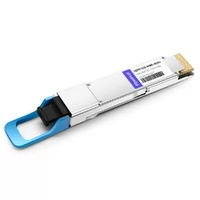
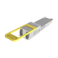
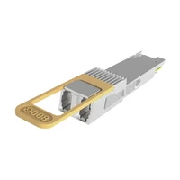
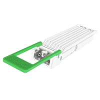
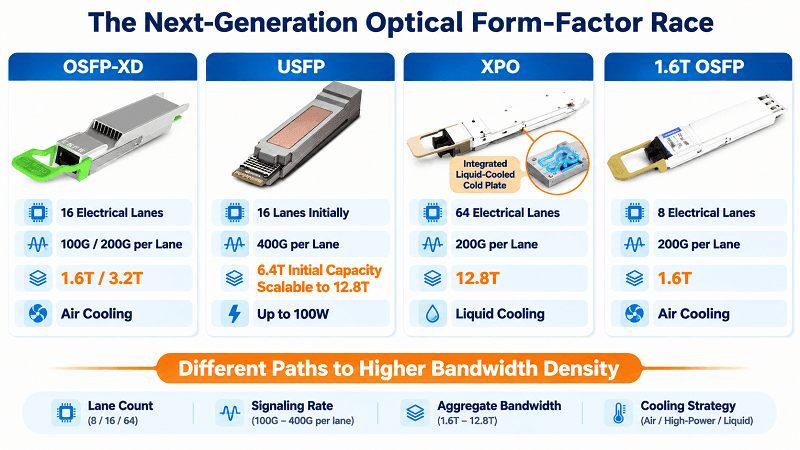
The lane-rate transition has triggered competition over what the next pluggable module will look like. Four form factors illustrate different approaches to increasing front-panel bandwidth density. Some are designed around 400G-per-lane signaling, while others increase capacity by using more lanes at 100G or 200G.
| Form factor | Backers / MSA | Electrical lanes | Per-lane rate | Aggregate capacity | Cooling |
| OSFP-XD | OSFP MSA | 16 | 100G or 200G | 1.6T or 3.2T | Heat sink / airflow |
| USFP | NVIDIA + Cisco | 16 initially; scalable to 32 | 400G | 6.4T initially; up to 12.8T | Supports up to 100W without a dedicated in-module cooling circuit |
| XPO | Arista-led XPO MSA | 64 | 200G PAM4 | 12.8T | Integrated liquid-cooled cold plate |
| QSFP-DD1600 | QSFP-DD MSA | 8 | 200G | 1.6T | Heat sink / airflow |
The key difference is how each form factor balances lane rate, lane count, density, and thermal design. OSFP-XD supports 16 electrical lanes and can scale from 1.6T at 100G per lane to 3.2T at 200G per lane. QSFP-DD1600 uses eight electrical lanes at 200G each for an aggregate capacity of 1.6T; it does not provide a 3.2T configuration in the current specification.
USFP is designed around 400G-per-lane electrical signaling. Its first planned transceivers use 16 full-duplex lanes for 6.4T, with a roadmap to 32 lanes and up to 12.8T. NVIDIA and Cisco state that USFP can support power dissipation of up to 100W without a separate, dedicated cooling circuit inside the transceiver. The system still needs an appropriate thermal design.
XPO takes a different approach. It uses 64 electrical lanes operating at 200G each to deliver 12.8T, and incorporates an integrated liquid-cooled cold plate designed to handle up to 400W per module. Rather than relying on 400G-per-lane signaling, XPO increases bandwidth density through a higher lane count and liquid cooling.
This is the same trade-off that appears throughout the broader next-generation optics discussion, and it connects directly to the co-packaged-optics question. For how pluggable optics compare with CPO and LPO at these rates, FiberMall’s OSFP roadmap tracks where the form factors are headed next.
What 400G per Lane Means for Your Optical Roadmap
For most network teams in 2026, 400G per lane is a planning horizon rather than an immediate purchasing decision. 200G-per-lane 1.6T modules are entering the market, although availability and platform validation vary by vendor and system. Meanwhile, 400G-per-lane technology is progressing through standards development, silicon implementation, and system validation.
Initial deployments may emerge around 2027, with broader volume adoption potentially extending into 2028–2029. These dates are industry outlooks, not guaranteed release schedules. Actual timing will depend on the completion of standards, the availability of compatible SerDes and switch silicon, thermal solutions, and multi-vendor validation.
Frequently Asked Questions
What does 400G per lane mean?
400G per lane means that one electrical lane or optical data channel carries a nominal data rate of 400 gigabits per second. In electrical-interface discussions, 448 Gb/s gross signaling is often used as a reference; if PAM4 is used, that corresponds to approximately 224 GBaud. On the optical side, a 400G lane refers to an optical channel carrying 400 Gb/s. The exact implementation depends on the interface.
What is the difference between electrical lanes and optical lanes?
Electrical lanes are the host-side SerDes signals between the switch or NIC and the transceiver. Optical lanes are independent data channels transmitted over fiber. Depending on the optical design, they may use parallel fibers or wavelength-division multiplexing. A DSP may include a gearbox function to map between different electrical and optical lane configurations, but the mapping varies by module architecture.
Is 400G per lane the same as 400G per lambda?
Not exactly. 400G per lambda specifically means that one optical wavelength carries 400 Gb/s. “400G per lane” is a broader term that can refer to an electrical SerDes lane or an optical data channel. An optical lane may correspond to a wavelength in a WDM system, but it can also be a parallel optical channel.
What is the next speed after 1.6T optics?
3.2T is the next aggregate-capacity step. Potential architectures include eight electrical lanes of 400G or sixteen electrical lanes of 200G. The 400G-per-lane approach can reach 3.2T with fewer electrical lanes, while a 16-lane 200G design uses a higher lane count. The appropriate architecture depends on the host interface, module form factor, optical design, and thermal requirements.
When will 400G-per-lane optical modules be available?
Initial deployments may emerge around 2027, with broader volume adoption potentially extending into 2028–2029. This remains a forecast rather than a confirmed industry-wide schedule. Standards development, compatible SerDes and switch silicon, module design, thermal management, and system validation all need to progress before broad commercial deployment.
How does PAM4 differ from NRZ?
NRZ encodes one bit per symbol using two signal levels. PAM4 encodes two bits per symbol using four levels, so it carries twice as much data at the same baud rate. The trade-off is a smaller separation between adjacent signal levels, which makes PAM4 more sensitive to noise and distortion. FEC and equalization are commonly used in high-speed PAM4 links, while the need for an in-module DSP depends on the transceiver architecture.
Related Products:
-
 QSFP-DD-400G-SR8 400G QSFP-DD SR8 PAM4 850nm 100m MTP/MPO OM3 FEC Optical Transceiver Module
$149.00
-
QSFP-DD-400G-VR4 400G QSFP-DD VR4 PAM4 850nm 50m MPO-12 OM4 FEC Optical Transceiver Module
$350.00
-
QSFP-DD-400G-DR4 400G QSFP-DD DR4 PAM4 1310nm 500m MTP/MPO SMF FEC Optical Transceiver Module
$400.00
-
QSFP-DD-400G-SR4 QSFP-DD 400G SR4 PAM4 850nm 100m MTP/MPO-12 OM4 FEC Optical Transceiver Module
$450.00
-
QSFP-DD-400G-FR4 400G QSFP-DD FR4 PAM4 CWDM4 2km LC SMF FEC Optical Transceiver Module
$500.00
-
QSFP-DD-400G-XDR4 400G QSFP-DD XDR4 PAM4 1310nm 2km MTP/MPO-12 SMF FEC Optical Transceiver Module
$550.00
-
LQSFP-DD-800G-DR8D 800G LPO QSFP-DD800 DR PAM4 1310nm 500m DOM Dual MPO-12 SMF Optical Transceiver Module
$1500.00
-
LQSFP-DD-800G-SR8D 800G SR8 LPO QSFP-DD 850nm 50m OM3 MMF 2xMPO-12 Optical Transceiver Module
$1300.00
-
LOSFP-800G-DR8D 800G LPO OSFP DR8 PAM4 1310nm 500m DOM Dual MTP/MPO-12 SMF Optical Transceiver Module
$1800.00
-
LOSFP-800G-SR8D LPO OSFP 8x100G SR8 PAM4 850nm 50m DOM Dual MPO-12 MMF Optical Transceiver Module
$1000.00
-
OSFP-800G-FR4 800G OSFP FR4 (200G per line) PAM4 CWDM Duplex LC 2km SMF Optical Transceiver Module
$3500.00
-
OSFP-800G-2FR2 800G OSFP 2FR2 (200G per line) PAM4 1291/1311nm 2km DOM Dual CS SMF Optical Transceiver Module
$2500.00