What makes Google’s TPU clusters stand out in the AI supercomputing race? How has the combination of 3D Torus topology and OCS (Optical Circuit Switching) technology enabled massive scaling while maintaining low latency and optimal TCO (Total Cost of Ownership)?
In this in-depth blog post, we dive deep into the evolution of Google’s TPU intelligent computing clusters, focusing on the synergistic mechanisms of 3D Torus topologies and OCS technology. Starting from the smallest topological unit—the 4x4x4 Cube—we reconstruct the standard 3D Torus in the TPUv4 4096 Pod and the Twisted 3D Torus in the TPUv7 9216 Pod. We’ll compare this with the cost-effective 2D Torus Mesh in TPUv5e/v6e, explore how Google achieves deterministic low latency at tens-of-thousands-chip scale, contrast with AWS and NVIDIA’s approaches, and look ahead to future trends like CPO (Co-Packaged Optics) enabling “chip-level light emission and all-optical direct connection.”
01 Prelude: Recap of TPU SuperNode Evolution
Previously, we explored the journey from TPUv1 (behind AlphaGo) to the OCS + ICI + 3D Torus-powered TPUv7 (9216-chip Ironwood super node), comparable to NVIDIA’s GB200/GB300. We also compared with Alibaba and NVIDIA, discussing who truly benefits in the AI era by both selling tools and mining gold.
Now, building on Google’s published papers about how 48 OCS units support a 4096-chip TPUv4 Pod, we’ll peel back the layers step-by-step: from the 4096-chip TPUv4 cluster to the latest 9216-chip TPUv7 cluster, highlighting the evolution of 2D/3D Torus + OCS optical switching + ICI networks, and how mature upstream/downstream supply chains complement this perfectly.
02 Foundation: TPUv4 and 3D Torus/OCS Implementation
The 4096-chip TPUv4 Pod is a landmark product showcasing mature application of Google’s OCS optical switching network—one of the few classic cases visible in public channels. Let’s build from the smallest module to the full cluster architecture.
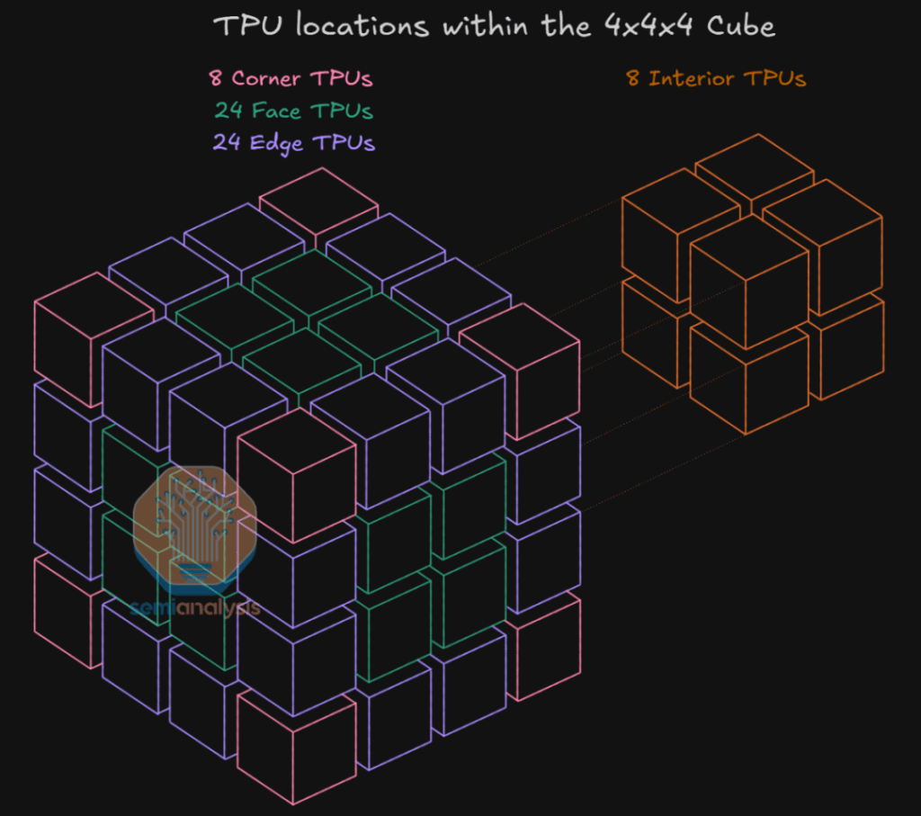
2.1 Smallest Topological Unit: 4×4×4 Cube
The minimal topological unit in Google TPUv4 Pod networking is the TPU Cube (or 4×4×4 Cube). Physically often a server cabinet, logically it’s a tightly integrated whole:
- Composition: 4 (X) × 4 (Y) × 4 (Z) = 64 TPU chips, resembling a solid fourth-order Rubik’s Cube.
- Links: Each TPU chip has 6 ICI (Inter-Chip Interconnect) high-speed links in ±X, ±Y, ±Z directions, forming the 3D Torus grid foundation.
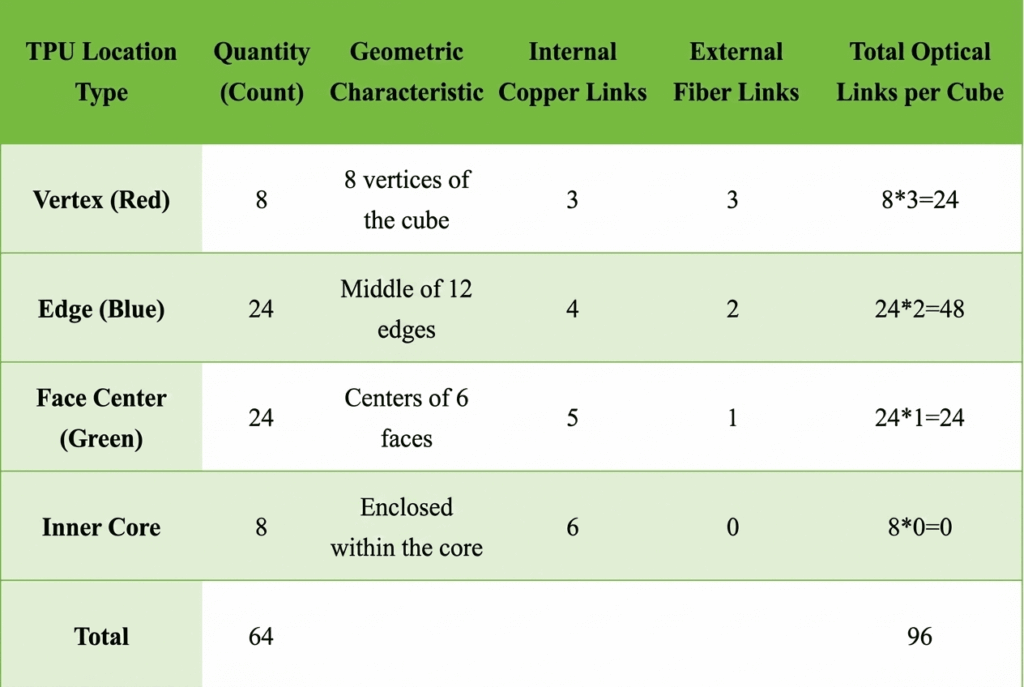
2.2 Link Layering and Optical-Electrical Boundaries in a Single Cube
In a standard 4×4×4 Cube, ICI links are divided into two categories based on position and medium, creating TPU’s unique hybrid optical-electrical network:
- Internal Interconnects (Cube Core): Internal links (core and non-exposed faces) use short PCB backplanes and copper cables for all-electrical signaling—no OCS, no optical conversion.
- External Interconnects (Cube Surface): Only links on the six outer surfaces are exposed, totaling 96 optical links per Cube connected to OCS for dynamic routing and massive scaling.
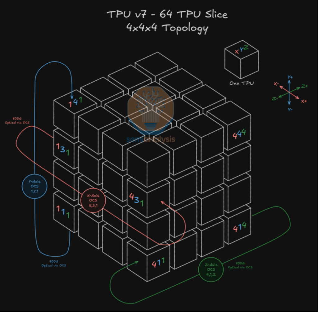
2.3 Deriving 48 OCS Units in TPUv4 Pod Cluster
From above, each Cube has 64 chips. For a 4096-chip Pod: 4096 / 64 = 64 Cubes.
Total optical links: 64 Cubes × 96 Links/Cube = 6144 links.
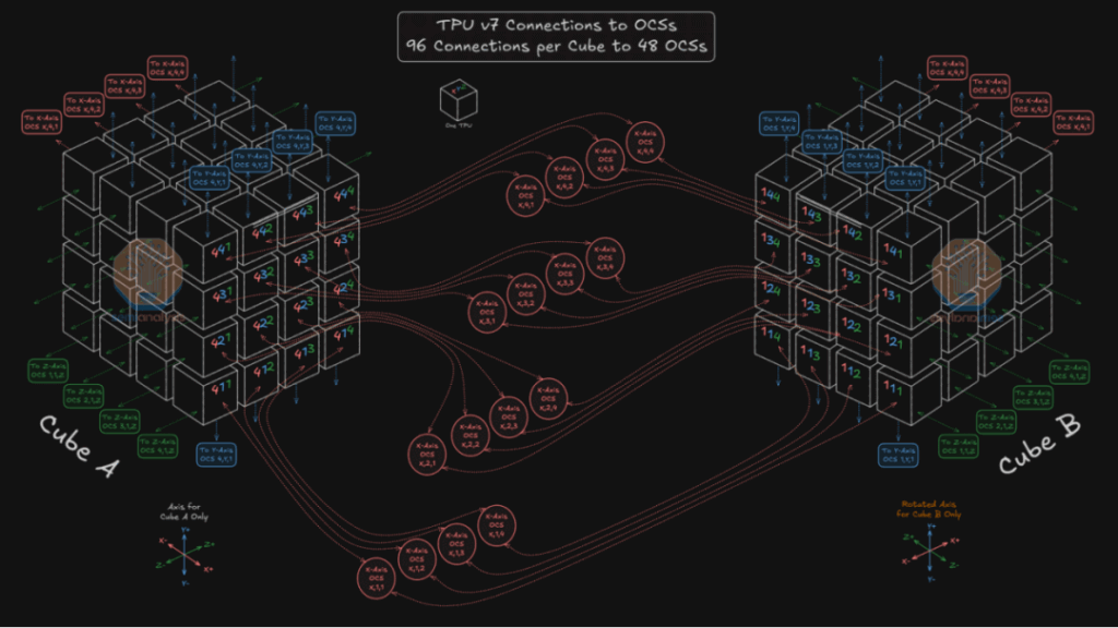
Google’s Palomar OCS is typically 136×136 ports, but engineered for 128 effective ports (binary alignment + 8 redundancy). Thus: 6144 Links ÷ 128 Ports/OCS = 48 OCS units.
To strictly align with 3D Torus, the 48 OCS are organized into three orthogonal groups for X/Y/Z traffic. For example, the X-axis group has 16 OCS, each handling only ±X face links across all Cubes under “same-dimension interconnect” principle—ensuring orthogonal isolation, simplifying routing algorithms, and avoiding deadlocks.
In 3D Torus, OCS acts as a massive dynamic patch panel, physically realizing Torus geometry. Data leaving a node’s X+ interface enters the adjacent node’s X- (step size 1 in standard TPUv4, variable N in twisted TPUv7). Edge nodes wrap around via OCS.
2.4 Core of TPUv4 Pod: Palomar OCS Microstructure
Unlike lossless packet switches, Palomar OCS doesn’t read headers or perform O/E conversion—it’s purely physical-layer “light reflection.”
Internal path forms a classic “W” shape to minimize insertion loss and enable any-to-any connectivity.
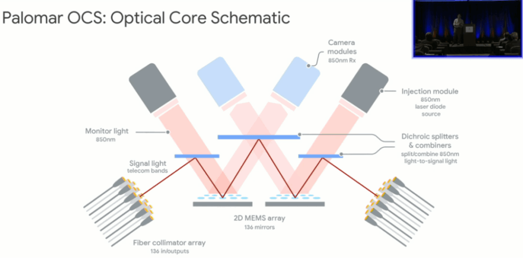
W-path: Collimator > Dichroic Mirror > 2D MEMS Array I > Dichroic Mirror > 2D MEMS Array II > Dichroic Mirror > Receiver Collimator.
Key components: Dual 2D MEMS for 3D beam steering; dichroic mirrors transmit 1310nm traffic while reflecting 850nm monitoring light. Paired with Injection + Camera modules for real-time in-band O&M and microsecond MEMS adjustments—this closed-loop alignment is a core barrier for Palomar OCS commercialization.
03 Architecture Evolution: Twisted 3D Torus and 2D Torus
With single-chip TDP rising to 600W and clusters exceeding 9,216 chips, TPUv7 (Ironwood) faces tougher cooling and latency challenges. Google introduced two major upgrades: twisted topology and extreme scale expansion.
3.1 TPUv7 Twisted 3D Torus Topology and 9216-Chip Derivation
TPUv7 Pod scales to 9216 chips vs. TPUv4’s 4096. Minimal unit remains 4x4x4 Cube (64 chips): 9216 / 64 = 144 Cubes.
Total links: 144 Cubes × 96 Links/Cube = 13,824 ports.
Google reportedly uses still 48 OCS units. (Figure 4 shows Cube A fanning out 96 links to 48 OCS.)
To handle this, OCS upgraded to 144×144 ports (matching 144 Cubes; likely 320×320 in reality), with Twisted 3D Torus links at 800G/1.6T for non-blocking communication.
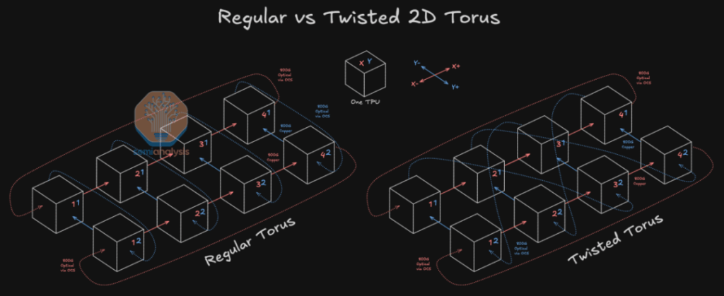
Topology upgrade: Introduces variable step size N for Twisted 3D Torus to reduce hops. Optimal N ≈ Dimension_Size / 2.
- Left: Standard 2D Torus (Step=1, sequential hops).
- Right: Twisted 2D Torus (Step=N, “wormhole” jumps via OCS).
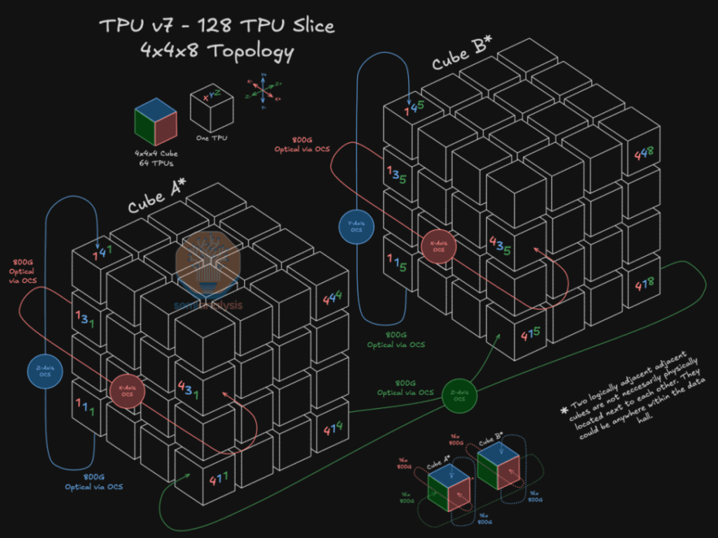
Extending to 3D: (Figure 6 shows 128 TPU Slice (4x4x8) connections, e.g., Z-axis jump from Cube A to Cube B.)
3.2 TPUv5e/v6e and 2D Torus Mesh
For latency-sensitive inference and mid-scale training, TPUv5e/v6e (Trillium) adopt cost-optimized design: Remove expensive OCS, use static 2D Torus Mesh.
Pod max 256 TPUs (4 liquid-cooled cabinets in 16×16 topology). Y-axis vertical via PCB/backplane; X-axis horizontal via QSFP-DD DAC copper cables, closing loops with long cables.
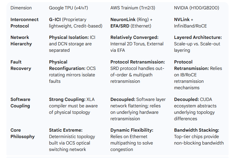
04 Industry Landscape Deep Comparison and Supply Chain Validation
4.1 Google (ICI) vs. AWS (Trainium) vs. NVIDIA
4.2 Industry Barriers: Why Hard to Replicate Google’s Model?
TPUv7 Pod’s moat is vertical integration from atoms to ecosystem:
- High-precision MEMS + closed-loop control crosses optics, mechanics, semiconductors—hard for general vendors.
- 3D Torus efficacy relies on Orion SDN + XLA compiler synergy for precise placement/routing.
- Full-stack: Chip + PyTorch XLA/JAX + TF/JAX + Gemini + billion-user apps—unreplicable data flywheel.
4.3 Supply Chain: Full Industrialization of OCS Ecosystem
Recent reports confirm Google’s OCS deployment via cross-validated supply chain:
- MEMS: Silex Microsystems mastered high-yield 2D MEMS.
- Integration: Accelink (192×192), Dekoli partnering Lumentum for 320×320.
- Optics: Tengjing for dichroic mirrors.
- Modules: Coherent/Zhongji for 800G/1.6T.
This ecosystem enables “Hardware as a Service” (HaaS): Long-life OCS as infrastructure, lowering TCO.
05 Future Evolution: Toward CPO and All-Optical Interconnect in Post-Moore Era
As TPUv8 advances with 224Gbps+ SerDes, traditional pluggable optics hit limits. CPO will break I/O boundaries.
Future Google TPU may shift to “chip-level light emission, all-optical direct”: Light engines co-packaged on TPU substrate, direct optical output to high-density backplane OCS (320×320+).
In post-Moore AGI era: Will universal Ethernet/InfiniBand win, or Google’s vertically integrated “walled garden” with photonics?
What aspects of Google’s TPU network evolution intrigue you most—the twisted torus reducing latency, the OCS supply chain maturity, or the potential shift to CPO? How do you see this comparing to competitors like NVIDIA’s NVLink optical future? Share your thoughts!
Related Products:
-
 NVIDIA MMA4Z00-NS Compatible 800Gb/s Twin-port OSFP 2x400G SR8 PAM4 850nm 100m DOM Dual MPO-12 MMF Optical Transceiver Module
$650.00
NVIDIA MMA4Z00-NS Compatible 800Gb/s Twin-port OSFP 2x400G SR8 PAM4 850nm 100m DOM Dual MPO-12 MMF Optical Transceiver Module
$650.00
-
NVIDIA MMA4Z00-NS-FLT Compatible 800Gb/s Twin-port OSFP 2x400G SR8 PAM4 850nm 100m DOM Dual MPO-12 MMF Optical Transceiver Module
$650.00
-
NVIDIA MMS4X00-NM Compatible 800Gb/s Twin-port OSFP 2x400G PAM4 1310nm 500m DOM Dual MTP/MPO-12 SMF Optical Transceiver Module
$900.00
-
NVIDIA MMS4X00-NM-FLT Compatible 800G Twin-port OSFP 2x400G Flat Top PAM4 1310nm 500m DOM Dual MTP/MPO-12 SMF Optical Transceiver Module
$1199.00
-
NVIDIA MMS4X50-NM Compatible OSFP 2x400G FR4 PAM4 1310nm 2km DOM Dual Duplex LC SMF Optical Transceiver Module
$1200.00
-
NVIDIA MMS4A20-XM800 Compatible 800G DR4 OSFP224 4x200G-PAM4 1311nm 500m RHS/Flat Top DOM MTP/MPO-12 APC InfiniBand XDR Transceiver Module
$1996.00
-
NVIDIA MMS4A00 (980-9IAH1-00XM00) Compatible 1.6T OSFP DR8D PAM4 1311nm 500m IHS/Finned Top Dual MPO-12 SMF Optical Transceiver Module
$2600.00
-
NVIDIA Compatible 1.6T 2xFR4/FR8 OSFP224 PAM4 1310nm 2km IHS/Finned Top Dual Duplex LC SMF Optical Transceiver Module
$3100.00
-
NVIDIA MMS4A00 (980-9IAH0-00XM00) Compatible 1.6T 2xDR4/DR8 OSFP224 PAM4 1311nm 500m RHS/Flat Top Dual MPO-12/APC InfiniBand XDR SMF Optical Transceiver Module
$3600.00
-
OSFP-1.6T-4FR2 1.6T OSFP 4FR2 PAM4 1291/1311nm 2km SN SMF Optical Transceiver Module
$22400.00
-
OSFP-1.6T-2FR4 1.6T OSFP 2xFR4 PAM4 2x CWDM4 2km Dual Duplex LC SMF Optical Transceiver Module
$22400.00
-
OSFP-1.6T-DR8D+ 1.6T OSFP DR8D+ PAM4 1311nm 2km Dual MPO-12 SMF Optical Transceiver Module
$18000.00