
What Is NVIDIA NVLink?
NVIDIA NVLink is a high-speed, low-latency interconnect that lets GPUs exchange data and access shared memory directly, without sending traffic through the PCIe bus and the CPU. NVIDIA designed it because PCIe could not keep pace with the memory demands of multi-GPU AI and HPC workloads, and its own overview of the technology frames NVLink as the glue that turns many GPUs into one accelerator. Across six generations, the aggregate bandwidth per GPU that NVLink supports has grown from 160 GB/s to 3.6 TB/s.
The term describes two things at once, and keeping them separate avoids most confusion. On consumer and workstation cards, NVLink is a physical bridge that joins two matching GPUs. On data-centre cards, NVLink is a switch-based fabric in which many GPUs behave as one large accelerator.
For a deeper look at how the fabric evolved from a simple ring to a rack-scale design, see the companion guide on NVLink and NVSwitch generations and topology.
NVLink, NVSwitch, and NVLink Switch
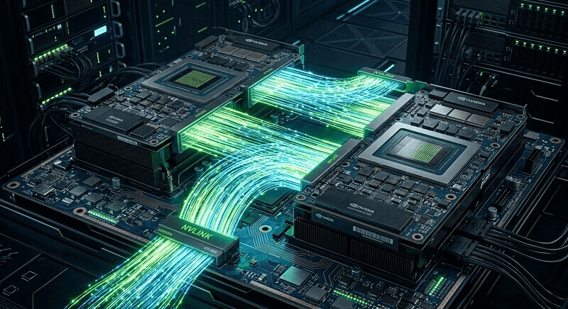
Three terms appear together often, so here is the short version:
- NVLink is the link itself, the point-to-point connection between two GPUs or between a GPU and a switch.
- NVSwitch is the switch ASIC that turns many NVLink links into an all-to-all fabric, so any GPU can reach any other at full bandwidth.
- NVLink Switch is the standalone 1U switch box that extends that fabric beyond a single server, connecting several GPU servers into one larger NVLink domain.
The three work as a stack. NVLink provides the lanes, NVSwitch provides the crossbar inside a server, and the NVLink Switch extends it across servers.
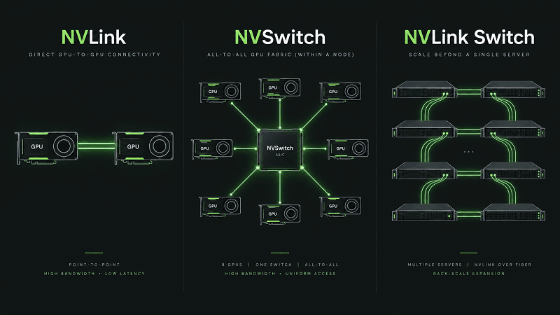
How NVLink Works: GPU-to-GPU Without PCIe
A traditional multi-GPU system routes data through PCIe switches on the motherboard, which is the path NVIDIA NVLink was built to bypass. That path adds latency and caps bandwidth, because a PCIe 5.0 lane carries 32 Gbps and a full x16 slot tops out near 128 GB/s. NVLink removes the bottleneck by giving GPUs a dedicated high-speed path to each other.
A modern NVLink link carries data using PAM4 signalling. Fourth-generation NVLink introduced 112G PAM4 SerDes, and each link is made up of two lanes. On an H100, 18 NVLink 4 links connect each GPU to the NVSwitch fabric, producing 900 GB/s of bidirectional bandwidth as follows:
- 112 Gbps per lane, two lanes per link, gives 224 Gbps unidirectional per link
- 224 Gbps equals 25 GB/s unidirectional, or 50 GB/s bidirectional per link
- 18 links at 50 GB/s each equal 900 GB/s bidirectional per GPU
That calculation is worth internalising, because every published NVLink figure follows the same convention: the headline number is the bidirectional aggregate per GPU, meaning transmit plus receive combined.
Two benefits follow from the direct path. First, GPUs can read and write each other’s memory in a unified address space, which is what makes model-parallel training practical: a model that exceeds one GPU’s memory can be split across several, because each GPU can reach the others’ memory directly. Second, the CPU and host memory drop out of GPU-to-GPU transfers entirely, so the interconnect carries the workload rather than the host bus. The result is that NVIDIA NVLink moves the traffic that matters, at consistent bandwidth, while PCIe continues to handle storage, networking, and host I/O.
What NVIDIA NVLink Is Used For
NVLink is not a general-purpose bus. It earns its cost in workloads that split a single job across many GPUs, so the most common uses are:
- Large language model training. Models with billions of parameters exceed any single GPU’s memory. NVLink lets tensor parallelism and pipeline parallelism shard the model across GPUs that exchange data at every step.
- Mixture-of-experts inference. MoE models route each token to a subset of experts, which means constant all-to-all traffic between GPUs. That traffic pattern is exactly what NVSwitch was designed to handle.
- HPC simulations. Climate, molecular dynamics, and fluid-dynamics codes exchange boundary data between GPUs on every timestep, where latency and bandwidth both matter.
- Distributed training at scale. Frameworks such as NCCL use NVLink for intra-node collective operations, then fall back to InfiniBand or Ethernet between nodes.
Where a workload does not need constant GPU-to-GPU communication, such as single-GPU inference or independent batch jobs, PCIe is sufficient and costs far less. NVIDIA NVLink pays off only when the interconnect sits on the critical path.
NVLink vs PCIe: Why the Interconnect Matters
The clearest way to see NVLink’s value is against PCIe, the general-purpose bus every server already has.
| Interconnect | Bandwidth | Best used for |
| PCIe 4.0 x16 | ~64 GB/s | Older general-purpose I/O |
| PCIe 5.0 x16 | ~128 GB/s | Current host-to-GPU and general I/O |
| PCIe 6.0 x16 | ~256 GB/s | Next-generation general I/O |
| NVLink 3 (A100) | 600 GB/s per GPU | Scale-up within a node |
| NVLink 4 (H100) | 900 GB/s per GPU | Scale-up within a node |
| NVLink 5 (B200) | 1.8 TB/s per GPU | Scale-up within a rack |
| NVLink 6 (Vera Rubin) | 3.6 TB/s per GPU | Scale-up across racks |
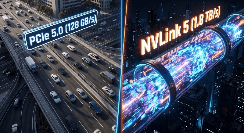
PCIe 5.0 delivers about 128 GB/s in each direction on a x16 slot, while NVLink 5 moves 1.8 TB/s per GPU in aggregate. That is roughly 14 times the bandwidth, with latency measured in fractions of a microsecond rather than microseconds. NVIDIA’s own summary describes the first generation as five to twelve times faster than PCIe, and the gap has widened with every generation since.
The difference matters most for workloads that exchange data constantly. Tensor parallelism, mixture-of-experts routing, and gradient synchronisation all move data between GPUs at every training step. On PCIe those transfers become the bottleneck; on NVLink they stay ahead of the compute.
NVLink Generations: Bandwidth From 1.0 to 6.0
NVLink has been revised roughly every two years, and each generation has raised the ceiling. The generational note matters because a card’s NVLink version is fixed by its GPU architecture, not by configuration. Each NVIDIA NVLink generation below is the first product to ship that version, and the published specification tracks every revision.
| Generation | Year | First GPU | Architecture | Bandwidth per GPU |
| NVLink 1 | 2016 | Tesla P100 | Pascal | 160 GB/s |
| NVLink 2 | 2017 | Tesla V100 | Volta | 300 GB/s |
| NVLink 3 | 2020 | A100 | Ampere | 600 GB/s |
| NVLink 4 | 2022 | H100 | Hopper | 900 GB/s |
| NVLink 5 | 2024 | B200 | Blackwell | 1.8 TB/s |
| NVLink 6 | 2026 | Vera Rubin | Rubin | 3.6 TB/s |
Why the Numbers Keep Doubling
Three things drove each jump: more links per GPU, faster signalling per link, and better switching.
- More links. The first generation used 4 links per GPU. Hopper and Blackwell use 18, and NVLink 6 supports up to 36.
- Faster signalling. Per-lane rates rose from 20 Gbps under NVLink 1 to 50 Gbps under NVLink 5, using PAM4 signalling that carries two bits per symbol.
- Better switching. NVSwitch arrived with the second generation, replacing the ring topology that could not connect GPUs across NUMA boundaries. Each NVSwitch generation has added capacity and, from NVSwitch 3, in-network reduction.
One caution when reading specifications: a shared generation number does not mean shared bandwidth. The consumer RTX 3090 and the data-centre A100 both use NVLink 3, yet the RTX 3090 delivers about 112.5 GB/s while the A100 delivers 600 GB/s. The consumer card devotes a single link pair to a bridge, while the data-centre card puts twelve links on a switch fabric.
NVLink-C2C: Chip-to-Chip NVLink
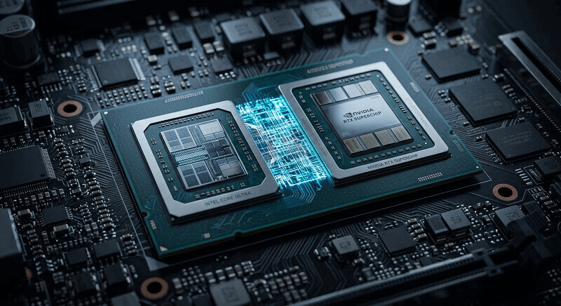
NVLink also exists in a die-level form called NVLink-C2C, short for chip-to-chip. Instead of linking two graphics cards, NVLink-C2C joins two processors inside a single package to form a superchip. It connects a Grace CPU to a Hopper or Blackwell GPU to make the Grace Hopper and Grace Blackwell superchips, and it links two Grace CPUs to make the Grace CPU Superchip. Because the dies sit on one package, NVLink-C2C runs at far higher bandwidth per pin than a board-level PCIe link and keeps the CPU and GPU cache-coherent. That coherency is what lets a Grace-Hopper system treat CPU memory and GPU memory as one addressable pool.
NVSwitch and NVLink Switch: Turning Links Into a Fabric
NVLink on its own is point-to-point, so a system of eight or more GPUs needs a switch to connect every card to every other card. That is the job of NVSwitch, the second half of the NVIDIA NVLink platform.
NVSwitch is a switch ASIC with NVLink ports on both sides. It creates a non-blocking, all-to-all crossbar, so every GPU in the domain can reach every other GPU at full bandwidth at the same time, with no relaying through neighbours. NVIDIA introduced NVSwitch with the DGX-2 in 2018 to connect 16 V100 GPUs, and the design has scaled with every generation. An 8-GPU HGX board carries several NVSwitch chips directly on the baseboard, which is how a DGX H100 behaves as one eight-GPU system.
From the third generation, NVSwitch also added in-network computing. The chip integrates SHARP, the Scalable Hierarchical Aggregation and Reduction Protocol, which aggregates results inside the switch during collective operations such as All-Reduce. Doing that in hardware cuts the number of network packets and speeds up the collective, which is the operation that dominates large-model training.
The NVLink Switch extends the fabric beyond one server. This is the 1U box announced alongside Hopper: it has 32 OSFP cages, two NVSwitch chips inside, and provides 128 NVLink 4 interfaces. With it, a fabric can span 256 H100 GPUs. The same principle scales up with Blackwell to the rack-scale NVL72 and beyond.
The deep dive on NVSwitch internals, transistor counts, and SHARP throughput lives in the NVLink and NVSwitch evolution guide. This page stays at the level of what each component does and when it matters.
NVLink in 2026: Blackwell, NVL72, and Vera Rubin
The NVIDIA NVLink story has moved two generations since this article first appeared in 2023. Here is where it stands now.
NVLink 5 and the Blackwell Generation
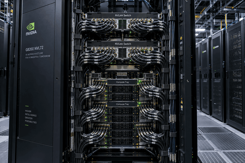
Blackwell brought NVLink 5 and NVSwitch 4, doubling per-GPU bandwidth to 1.8 TB/s. The headline system is the GB200 NVL72, which packs 72 Blackwell GPUs and 36 Grace CPUs into a single rack connected by nine NVSwitch trays. The rack acts as one GPU domain with roughly 130 TB/s of GPU-to-GPU bandwidth and about 13 TB of unified HBM memory. GB300 Blackwell Ultra extends the same platform through 2026 and moves the scale-out network to 800G ConnectX-8.
NVLink 6 and Vera Rubin
Vera Rubin brings NVLink 6, which doubles per-GPU bandwidth again to 3.6 TB/s across as many as 36 links. The first system, Vera Rubin NVL144, is scheduled to ship in the second half of 2026, with co-packaged optics on the roadmap for Rubin Ultra. For anyone planning cabling, this is the transition to watch, because NVLink 6 pushes more of the fabric onto high-speed optical and active electrical links.
NVLink Fusion
NVIDIA’s NVLink Fusion program opens the NVLink fabric to partner silicon, letting third-party CPUs and accelerators join an NVLink domain. It signals that NVLink is becoming a platform rather than a feature of NVIDIA’s own systems.
The Consumer Story Ended at the RTX 3090
One fact about NVLink in 2026 surprises many readers: NVIDIA removed it from GeForce after the RTX 3090. The RTX 40-series (Ada, 2022) and RTX 50-series (Blackwell, 2025) have no NVLink connector. NVLink now survives only where memory sharing drives the workload, which means professional, workstation, and data-centre silicon. The NVLink compatible cards list covers the consumer and workstation exceptions in full.
What NVLink Means for Cabling
NVLink is often described as if it were wireless. In practice it is a physical fabric, and the medium changes at the rack boundary. That boundary is what determines the transceivers, DAC cables, and fiber a cluster needs.
Inside the Rack: Copper NVLink
Within a rack, NVLink runs on copper. The GB200 NVL72 uses short twin-axial copper assemblies at the rear of the cabinet because the runs are under a few metres and the power saving is large; running that fabric optically would add roughly 20 kW per rack. These runs behave like oversized DAC cables and plug directly into the compute and NVSwitch trays.
Between Racks: Optics
Where an NVLink domain crosses a rack boundary, the NVSwitch trays connect through OSFP cages carrying real NVLink traffic. The two-cabinet GB200 NVL36x2 uses 1.6T OSFP for that link. Beyond NVLink, the scale-out network that carries jobs and storage between racks runs on InfiniBand or Ethernet optics: 400G ConnectX-7 on DGX H100, 800G ConnectX-8 on GB300, and Quantum-X800 or Spectrum-X800 switches.
The practical rule is simple. Keep NVLink on copper where the distance is short and the power budget is tight, and use 800G and 1.6T OSFP optics for rack-to-rack and scale-out links. A useful sizing reference is our guide to how many optical transceivers a GPU cluster needs.
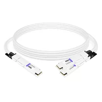
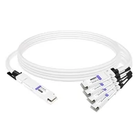
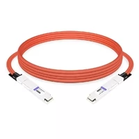
For the optical and copper layer, FiberMall builds NVIDIA-compatible modules across each tier. The 800G OSFP SR8 module covers short-reach scale-out and NVLink fabrics, while 800G NDR DAC cables handle the short copper hops.
The rest of the lineup maps directly onto the fabric layers:
- 800G OSFP DR8 modules for 500m single-mode scale-out runs
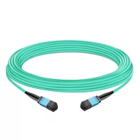
- MPO fiber trunks for structured cabling between racks
- 1.6T OSFP modules for the transition to Vera Rubin
Frequently Asked Questions
What is NVIDIA NVLink?
NVIDIA NVLink is a high-speed interconnect that connects GPUs directly so they can share data and memory without going through PCIe or the CPU. In the current Blackwell generation it delivers up to 1.8 TB/s of bidirectional bandwidth per GPU, roughly 14 times a PCIe 5.0 x16 slot.
How fast is NVLink?
NVLink 5 on Blackwell moves 1.8 TB/s per GPU in aggregate. The generations before it delivered 160 GB/s (NVLink 1), 300 GB/s (NVLink 2), 600 GB/s (NVLink 3), and 900 GB/s (NVLink 4). NVLink 6 arrives with Vera Rubin in 2026 at 3.6 TB/s per GPU.
Is NVLink faster than PCIe?
Yes. NVLink 5 provides 1.8 TB/s per GPU against about 128 GB/s for a PCIe 5.0 x16 slot, which is roughly 14 times the bandwidth. NVLink also lowers latency to fractions of a microsecond and bypasses host memory for GPU-to-GPU traffic.
What is the difference between NVLink and NVSwitch?
NVLink is the point-to-point link between two GPUs. NVSwitch is the switch chip that connects many NVLink links into an all-to-all fabric, so every GPU in a domain can talk to every other GPU at full bandwidth. NVSwitch is what turns a group of GPUs into one system.
Do RTX 40-series and RTX 50-series cards support NVLink?
No. NVIDIA removed NVLink from GeForce after the RTX 3090. The RTX 40-series and RTX 50-series have no NVLink connector. NVLink remains in workstation and data-centre GPUs such as the RTX PRO 6000 Blackwell, A100, H100, H200, B200, GB200, and GB300.
What cables does an NVLink system need?
Copper inside the rack, optics between racks. An NVL72 uses short high-speed copper NVLink assemblies to link compute trays to NVSwitch trays, then 800G or 1.6T OSFP optics and DAC or AEC cables for rack-to-rack and scale-out connections.
Conclusion
NVIDIA NVLink is the interconnect that made multi-GPU computing practical. It began as a 160 GB/s point-to-point link for four Pascal GPUs, added NVSwitch to build fabrics, and now spans 72-GPU racks at roughly 130 TB/s. In 2026 it sits at NVLink 5 on Blackwell, with NVLink 6 and Vera Rubin arriving in the second half of the year.
The essentials to carry away:
- NVLink is a direct GPU-to-GPU interconnect. It removes PCIe and the CPU from GPU traffic, which is why model-parallel AI training depends on it.
- Bandwidth is set by generation. 160 GB/s on NVLink 1 up to 3.6 TB/s on NVLink 6, and a shared generation number does not mean shared bandwidth.
- NVSwitch turns links into a fabric. It creates the all-to-all crossbar that lets many GPUs act as one.
- Consumer NVLink ended at the RTX 3090. Current NVLink lives in workstation and data-centre GPUs.
- The physical layer splits at the rack. Copper inside, 800G and 1.6T OSFP optics between racks.
If you are planning the connectivity for an NVIDIA GPU cluster, start with the optical layer. FiberMall’s 800G OSFP DR8 modules cover the single-mode scale-out links, and the companion NVLink compatible cards guide matches each GPU to the cabling it needs. To align modules with your switches, network cards, and NVLink fabric, our engineers can help on the FiberMall questions page.
Related Products:
-
 NVIDIA MMA4Z00-NS400 Compatible 400G OSFP SR4 Flat Top PAM4 850nm 30m on OM3/50m on OM4 MTP/MPO-12 Multimode FEC Optical Transceiver Module
$400.00
NVIDIA MMA4Z00-NS400 Compatible 400G OSFP SR4 Flat Top PAM4 850nm 30m on OM3/50m on OM4 MTP/MPO-12 Multimode FEC Optical Transceiver Module
$400.00
-
NVIDIA MMA4Z00-NS-FLT Compatible 800GBASE 2 x SR4/SR8 OSFP RHS/Flat Top PAM4 850nm 100m DOM Dual MPO-12 MMF Optical Transceiver Module
$600.00
-
NVIDIA MMA4Z00-NS Compatible 800GBASE 2 x SR4/SR8 OSFP PAM4 850nm 100m DOM Dual MPO-12 MMF Optical Transceiver Module
$550.00
-
NVIDIA MMS4X00-NM Compatible 800GBASE 2 x DR4/DR8 OSFP IHS/Closed Finned Top PAM4 1310nm 500m DOM Dual MTP/MPO-12 SMF Optical Transceiver Module
$600.00
-
NVIDIA MMS4X00-NM-FLT Compatible 800GBASE 2 x DR4/DR8 OSFP Flat Top PAM4 1310nm 500m DOM Dual MTP/MPO-12 SMF Optical Transceiver Module
$650.00
-
NVIDIA MMS4X00-NS400 Compatible 400G OSFP DR4 Flat Top PAM4 1310nm MTP/MPO-12 500m SMF FEC Optical Transceiver Module
$450.00
-
NVIDIA(Mellanox) MMA1T00-HS Compatible 200G Infiniband HDR QSFP56 SR4 850nm 100m MPO-12 APC OM3/OM4 FEC PAM4 Optical Transceiver Module
$139.00
-
NVIDIA MFP7E10-N010 Compatible 10m (33ft) 8 Fibers Low Insertion Loss Female to Female MPO Trunk Cable Polarity B APC to APC LSZH Multimode OM3 50/125
$47.00
-
NVIDIA MCP7Y00-N003-FLT Compatible 3m (10ft) 800G Twin-port OSFP to 2x400G Flat Top OSFP InfiniBand NDR Breakout DAC
$260.00
-
NVIDIA MCP7Y70-H002 Compatible 2m (7ft) 400G Twin-port 2x200G OSFP to 4x100G QSFP56 Passive Breakout Direct Attach Copper Cable
$155.00
-
NVIDIA MCA4J80-N003-FTF Compatible 3m (10ft) 800G Twin-port 2x400G OSFP to 2x400G OSFP InfiniBand NDR Active Copper Cable, Flat top on one end and Finned top on other
$600.00
-
NVIDIA MCP7Y10-N002 Compatible 2m (7ft) 800G InfiniBand NDR Twin-port OSFP to 2x400G QSFP112 Breakout DAC
$190.00