In the world of AI acceleration, the battle between Google’s Tensor Processing Unit (TPU) and NVIDIA’s GPU is far more than a spec-sheet war — it’s a philosophical clash between custom-designed ASIC (Application-Specific Integrated Circuit) and general-purpose parallel computing (GPGPU). These represent the two dominant schools of thought in today’s AI hardware landscape.
This in-depth blog post compares them across architecture, performance, software ecosystem, interconnect scaling, and business model — everything you need to know in 2025.
Core Design Philosophy
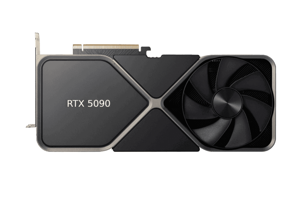
NVIDIA GPU: The King of General-Purpose Parallel Computing
Origin: Born for graphics rendering (gaming), evolved into universal parallel computing via CUDA.
Core Architecture: SIMT (Single Instruction, Multiple Threads) with thousands of small CUDA cores.
Superpower: Extreme flexibility — it excels not only at AI matrix math but also scientific computing, ray tracing, cryptocurrency mining, and more.
Trade-off: To maintain universality, GPUs carry complex control logic (branch prediction, cache hierarchy, etc.), which consumes die area and power.
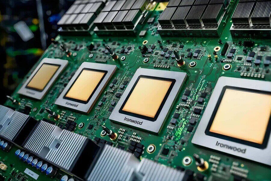
Google TPU: The Ultimate AI “Specialist”
- Origin: Custom-built by Google to handle exploding internal AI workloads (Search, Translate, AlphaGo, Gemini, etc.).
- Core Architecture: Systolic Array — the beating heart of TPU.
- Analogy: While CPU/GPU act like delivery workers running back and forth to memory, TPU’s systolic array works like a factory assembly line. Data pulses through thousands of ALUs like blood in veins, reused hundreds of times before being written back.
- Laser Focus: Optimized exclusively for matrix multiplication — the operation that accounts for >90% of compute in Transformers, CNNs, and most modern neural networks.
- Result: Under the same process node, TPU achieves dramatically higher silicon efficiency and performance-per-watt.
Memory, Bandwidth & Scaling Interconnect
Memory Bandwidth (HBM)
- NVIDIA: Extremely aggressive. The H100, H200, and Blackwell B200 series have essentially reserved most of SK hynix’s top-bin HBM3e production. NVIDIA’s philosophy = “brute-force the memory wall with insane bandwidth.”
- Google TPU: More conservative but sufficient. Thanks to extremely high data reuse inside the systolic array, TPUs need less external memory bandwidth than you’d expect.
Cluster Scaling — Google’s Secret Weapon
When training ultra-large models (GPT-4, Gemini Ultra, etc.), single-card performance is no longer the bottleneck — interconnect efficiency is.
| Aspect | NVIDIA (NVLink + InfiniBand/Quantum-2) | Google TPU (ICI + OCS) |
| Interconnect type | External high-end switches & NICs | On-die ICI (Inter-Chip Interconnect) + Optical Circuit Switches |
| Topology | Fat-tree with NVSwitch | 2D/3D Torus + dynamically reconfigurable optical switching |
| Cost & Complexity | Extremely expensive and complex cabling | Dramatically lower cost, simpler deployment |
| Reconfigurability | Static during job | Can reconfigure thousands of TPUs in seconds |
| Scaling Winner | Excellent but pricey | Often superior linear scaling at 10,000+ chip scale |
Google’s Optical Circuit Switch (OCS) technology is a game-changer: it can physically rewire the network topology in seconds, achieving near-perfect bisection bandwidth at massive scale.
Software Ecosystem — NVIDIA’s Deep Moat
NVIDIA CUDA: The Undisputed “English of AI”
- Almost every major framework (PyTorch, TensorFlow, JAX, etc.) is developed and optimized first on CUDA.
- Dynamic graphs, easy debugging, millions of Stack Overflow answers — researchers love it.
- “Just works” experience for 99% of use cases.
Google XLA + JAX/PyTorch-XLA: The Fast Follower
- TPU code must be compiled via XLA (Accelerated Linear Algebra).
- Originally tightly coupled with TensorFlow; now aggressively supporting JAX and PyTorch/XLA.
- Challenges:
- Mostly static-graph: heavy control flow (lots of if/else) can kill performance or even fail compilation.
- Debugging is painful — cryptic compiler errors with far fewer community resources.
- Superpower: Once compiled, XLA performs extreme operator fusion, often achieving higher MFU (Model FLOPs Utilization) than hand-tuned CUDA code.
Performance Comparison (2025 Latest Generation)
| Metric | NVIDIA (H100 / Blackwell) | Google TPU v5p / v6 (Trillium) | Winner |
| Single-card raw FLOPS (FP8/FP16) | Higher peak | Slightly lower peak | NVIDIA |
| Small / research models | Significantly faster | Slower due to compilation | NVIDIA |
| Large-scale training MFU | 45–55% (optimized) | 55–65%+ | Google TPU |
| Linear scaling (10k+ chips) | Very good but expensive | Often better & cheaper | Google TPU |
| Low-latency inference | TensorRT-LLM king | Good but not best | NVIDIA |
| High-throughput inference | Excellent | TPU v5e/v6 extremely cost-effective | Google (cost) |
Bottom line:
- For research, prototyping, or latency-critical inference → NVIDIA wins.
- For training and serving frontier-scale models at Google-scale efficiency → TPU often wins on both performance and cost.
Business Model & Availability — The Fundamental Difference
| Company | Analogy in PC Era | Business Style | Availability |
| NVIDIA | Intel | Sells the “best shovels” to everyone during the gold rush | Open market, anyone with money can buy |
| Apple | Vertically integrated, keeps the best hardware for itself | Primarily Google Cloud (some partner access) |
NVIDIA dominates the entire pyramid from gamers → startups → hyperscalers. Google TPU is mostly reserved for Google’s own services and Google Cloud customers, giving them a structural cost advantage that is extremely hard to compete with.
Final Verdict in 2025
- If you are an independent lab, startup, or need maximum flexibility and ecosystem support → NVIDIA GPU + CUDA remains the default choice.
- If you are running planet-scale models and care about total cost of ownership at 100,000+ accelerator scale → Google TPU (especially v6 Trillium) is increasingly unbeatable.
The war is far from over. NVIDIA is pushing Blackwell and NVLink 6; Google just announced TPU v6 “Trillium” with 4.7× performance per chip over v5p. The next 2–3 years will be epic.
Related Products:
-
 NVIDIA MMA4Z00-NS400 Compatible 400G OSFP SR4 Flat Top PAM4 850nm 30m on OM3/50m on OM4 MTP/MPO-12 Multimode FEC Optical Transceiver Module
$550.00
NVIDIA MMA4Z00-NS400 Compatible 400G OSFP SR4 Flat Top PAM4 850nm 30m on OM3/50m on OM4 MTP/MPO-12 Multimode FEC Optical Transceiver Module
$550.00
-
NVIDIA MMS4X00-NS400 Compatible 400G OSFP DR4 Flat Top PAM4 1310nm MTP/MPO-12 500m SMF FEC Optical Transceiver Module
$700.00
-
NVIDIA MMA1Z00-NS400 Compatible 400G QSFP112 VR4 PAM4 850nm 50m MTP/MPO-12 OM4 FEC Optical Transceiver Module
$550.00
-
NVIDIA MMS1Z00-NS400 Compatible 400G NDR QSFP112 DR4 PAM4 1310nm 500m MPO-12 with FEC Optical Transceiver Module
$850.00
-
NVIDIA MMA4Z00-NS Compatible 800Gb/s Twin-port OSFP 2x400G SR8 PAM4 850nm 100m DOM Dual MPO-12 MMF Optical Transceiver Module
$650.00
-
NVIDIA MMA4Z00-NS-FLT Compatible 800Gb/s Twin-port OSFP 2x400G SR8 PAM4 850nm 100m DOM Dual MPO-12 MMF Optical Transceiver Module
$650.00
-
NVIDIA MMS4X00-NM Compatible 800Gb/s Twin-port OSFP 2x400G PAM4 1310nm 500m DOM Dual MTP/MPO-12 SMF Optical Transceiver Module
$900.00
-
NVIDIA MMS4X00-NM-FLT Compatible 800G Twin-port OSFP 2x400G Flat Top PAM4 1310nm 500m DOM Dual MTP/MPO-12 SMF Optical Transceiver Module
$1199.00
-
NVIDIA MMS4X50-NM Compatible OSFP 2x400G FR4 PAM4 1310nm 2km DOM Dual Duplex LC SMF Optical Transceiver Module
$1200.00
-
NVIDIA MMS4A00 (980-9IAH1-00XM00) Compatible 1.6T OSFP DR8D PAM4 1311nm 500m IHS/Finned Top Dual MPO-12 SMF Optical Transceiver Module
$2600.00
-
NVIDIA Compatible 1.6T 2xFR4/FR8 OSFP224 PAM4 1310nm 2km IHS/Finned Top Dual Duplex LC SMF Optical Transceiver Module
$3100.00
-
NVIDIA MMS4A00 (980-9IAH0-00XM00) Compatible 1.6T 2xDR4/DR8 OSFP224 PAM4 1311nm 500m RHS/Flat Top Dual MPO-12/APC InfiniBand XDR SMF Optical Transceiver Module
$3600.00