GB200 Interconnect Architecture Analysis
NVLink Bandwidth Calculation
NVIDIA has a lot of confusion in the calculation of NVLink transmission bandwidth and the concepts of SubLink/Port/Lane. Typically, the NVLink bandwidth of a single B200 chip is 1.8TB/s. This is usually calculated using the memory bandwidth algorithm, with the unit being bytes per second (B/s). However, on the NVLink Switch or IB/Ethernet switches and network cards, the perspective is from Mellanox, who calculates the network bandwidth in bits per second (b/s). Let’s explain the NVLink calculation method in detail. Starting from NVLink 3.0, four differential pairs form a “sub-link” (NVIDIA often uses the terms Port/Link, with a somewhat vague definition). These 4 pairs of differential signal lines contain both the receive and transmit direction signals. When calculating network bandwidth, a 400Gbps interface typically refers to the ability to transmit and receive 400Gbps of data simultaneously.
It is composed of a total of 4 pairs of differential signal lines, with 2 pairs each for RX and TX. From the network’s perspective, it is a unidirectional 400Gbps link, while from the memory bandwidth perspective, it supports a memory access bandwidth of 100GB/s.
NVLINK 5.0 Interconnect Bandwidth
The Blackwell generation uses 224G Serdes, with a sub-link transmission rate of 200Gbps * 4 (4 differential pairs) / 8 = 100GB/s, and a single-direction network bandwidth of 400Gbps. The B200 has 18 sub-links, resulting in a bandwidth of 100GB/s * 18 = 1.8TB/s, which is equivalent to 9 single-direction 400Gbps interfaces from a network perspective. Similarly, the NVSwitch introduction mentions that Dual 200Gb/sec SerDes make up a 400Gbp
s Port.
For the sake of clarity, we define the following terms:
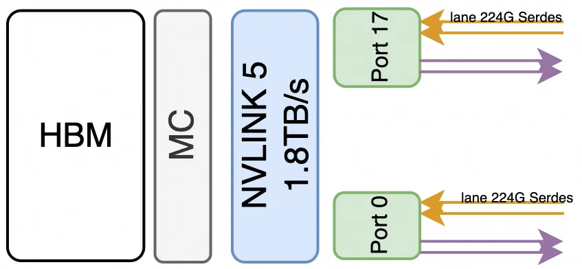
B200 NVLINK bandwidth is 1.8TB/s, composed of 18 Ports, each at 100GB/s, made up of four differential pairs, with each Port containing two 224Gbps Serdes (2x224G PAM4 equates to 400Gbps single-direction bandwidth per Port).
NVLINK 4.0 Interconnect
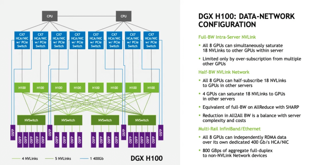
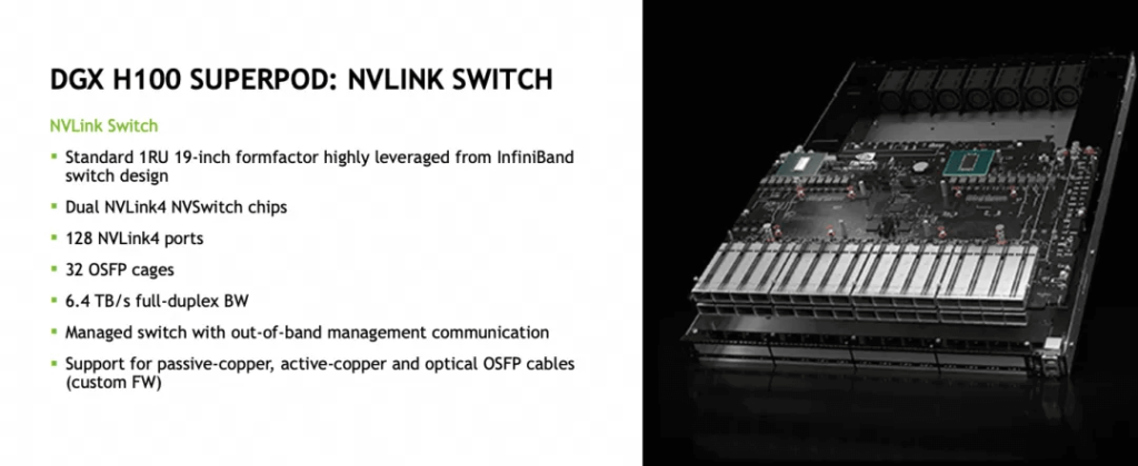
Regarding Hopper, NVLINK 4.0 uses 112G Serdes, with a single differential signal line capable of 100Gbps, resulting in a cumulative single NVLINK Sub-link of 4x100Gbps = 50GB/s. Hopper products supporting NVLINK 4.0 have 18 sub-links (ports), so a single H100 supports 50GB/s * 18 = 900GB/s. A single system with 8 cards can utilize 4 NVSwitches for connectivity, as shown in the image.
It is also possible to add a second-level switch to create a 256-card cluster.
The expansion interface uses OSFP optical modules, which can support 16 differential signal lines, allowing a single OSFP to support 4 NVLINK Ports.
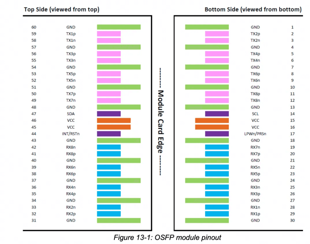
The NVLink Switch in the image contains 32 OSFP optical module connectors, supporting a total of 32 * 4 = 128 NVLINK 4 Ports.
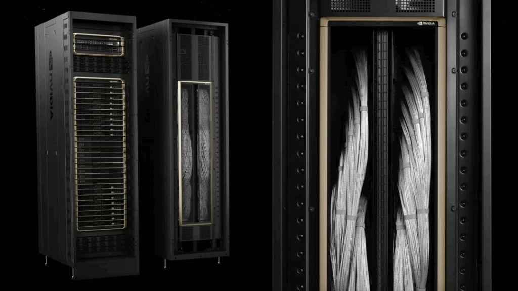
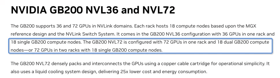
GB200 NVL72
The GB200 NVL72 system has the following specifications, with the main focus being on the NVLINK interconnect:
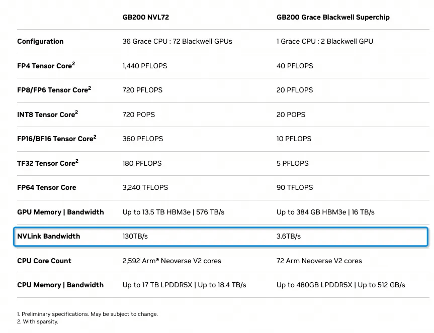
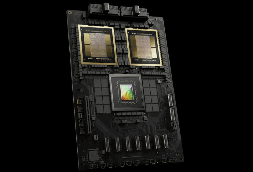
Each GB200 contains one 72-core Grace ARM CPU and two Blackwell GPUs.
The entire system is composed of Compute Trays and Switch Trays. Each Compute Tray contains two GB200 subsystems, totaling 4 Blackwell GPUs.
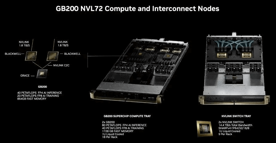
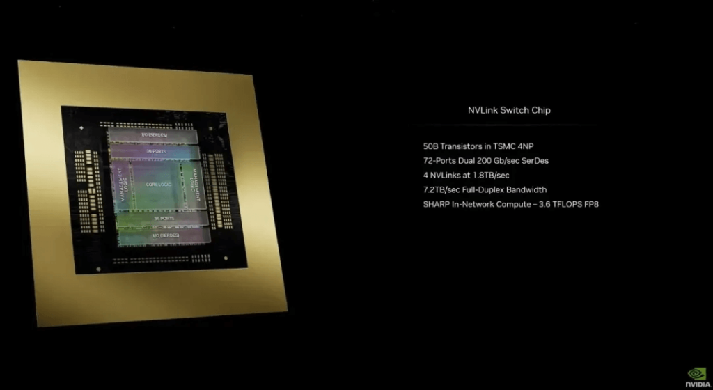
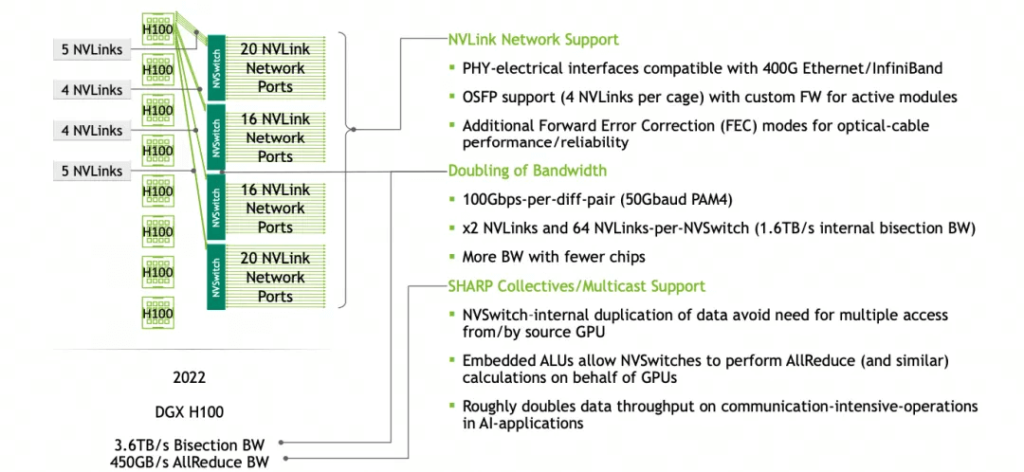
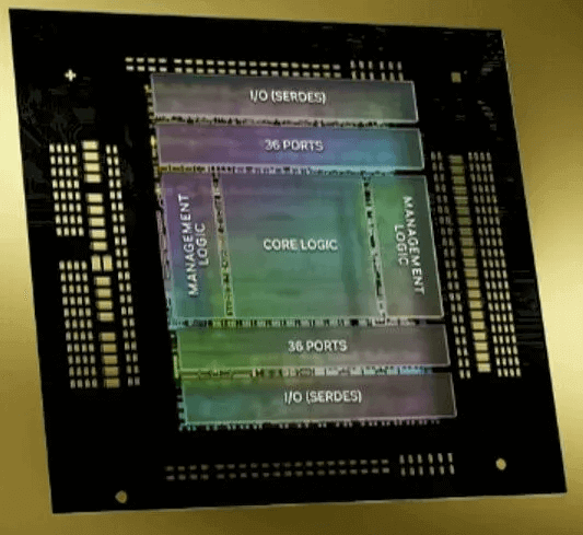
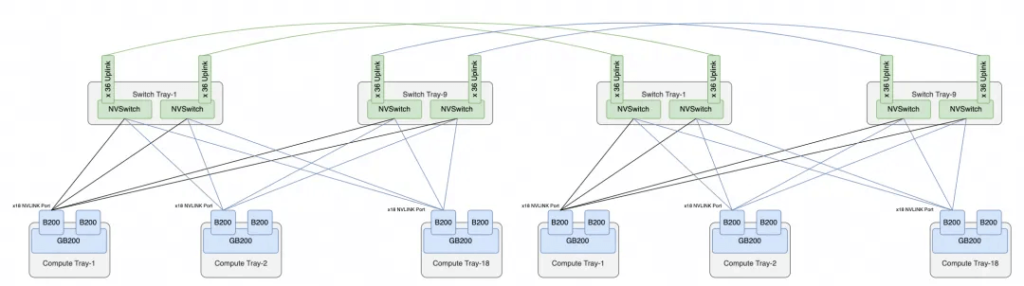
Each Switch Tray contains two NVLINK Switch chips, providing a total of 72 * 2 = 144 NVLINK Ports. The internal structure of a single switch chip is shown, with 36 ports on the top and bottom, providing 7.2TB/s of bandwidth. Using network calculations, this equates to 28.8Tbps of switching capacity, slightly less than the current leading 51.2Tbps switch chip, but this is due to the implementation of SHARP (NVLS) functionality.
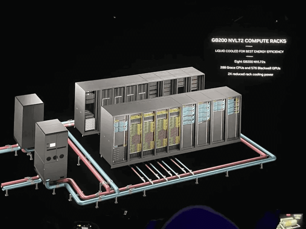
The entire rack supports 18 Compute Trays and 9 Switch Trays, forming the NVL72 architecture with 72 fully interconnected Blackwell chips.
Each GB200 subsystem has 2 * 18 = 36 NVLink5 Ports. The external interconnect of the system does not use OSFP optical modules, but rather a direct copper backplane connection, as shown in the diagram.
The overall NVL72 interconnect topology is as follows:
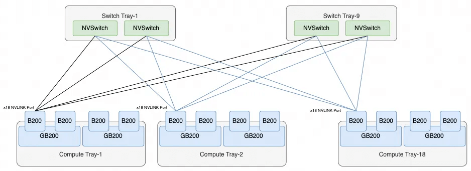
Each B200 has 18 NVLINK Ports, and there are 18 NVLINK Switch chips across the 9 Switch Trays. Therefore, each B200’s ports connect to one NVSwitch chip, resulting in a total of 72 Ports per NVSwitch, which is how the NVL72 system fully connects all 72 B200 chips.
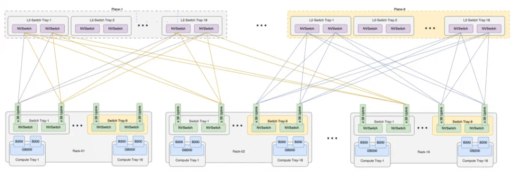
NVL576
We notice that in the NVL72 cabinet, all the switches no longer have additional interfaces to form a larger two-tier switch cluster. From the official NVIDIA images, 16 cabinets are arranged in two rows, and although the total is exactly 72 * 8 = 576 cards liquid-cooled cluster, the connection cables between the cards seem to be more through the Scale-Out RDMA network interconnect, rather than the Scale-Up NVLINK network interconnect.
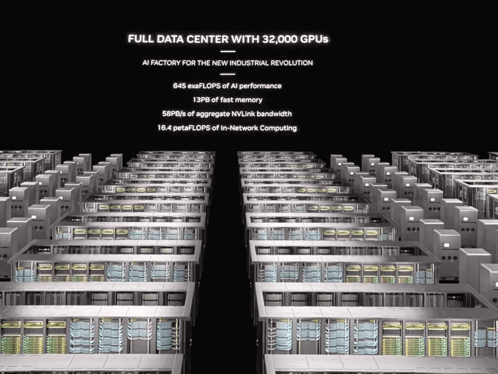
For a 32,000-card cluster, it is also through such NVL72 cabinets, one row of 9 cabinets, 4 NVL72 and 5 network cabinets, two rows of 18 cabinets forming a Sub-Pod, and connected through the RDMA Scale-Out network.
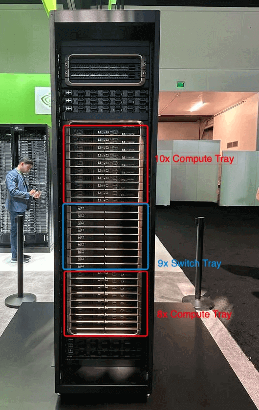
Of course, this is not the so-called NVL576. If NVL576 is required, each 72 GB200 needs to be configured with 18 NVSwitches, which would not fit in a single cabinet. We notice that the official has mentioned that there is a single-cabinet version of NVL72, as well as a dual-cabinet version, and in the dual-cabinet version, each Compute Tray only has one GB200 subsystem.
On the other hand, we notice that there are spare copper cable connectors on the NVSwitch, which are likely customized for different copper backplane connections.
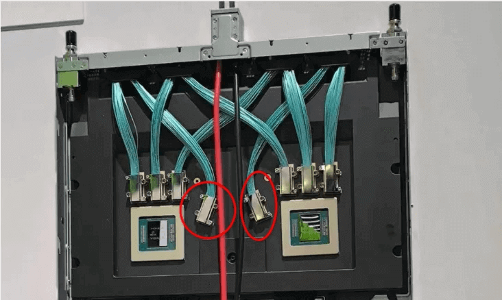
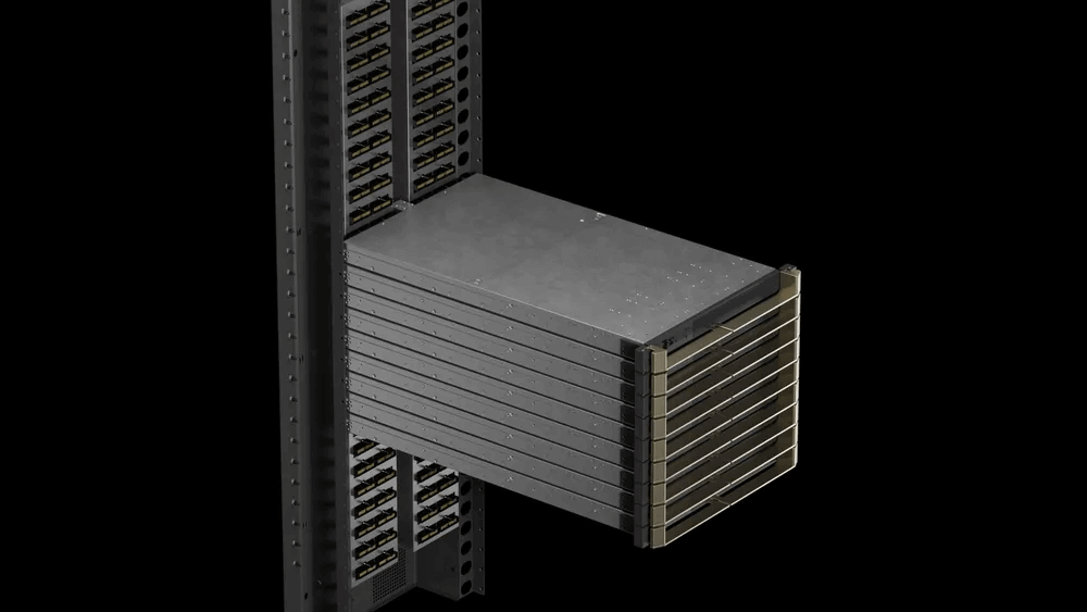
It is unknown whether these interfaces will have additional OSFP Cages above the copper interconnect backplane for second-tier NVSwitch interconnect, but this method has one advantage: the single-cabinet version is non-scalable, while the dual-cabinet version is scalable, as shown in the image.
The dual-cabinet version has 18 NVSwitch Trays, which can be interconnected back-to-back to form NVL72. Although the number of switches has doubled, each switch provides 36 uplink ports for future expansion to the 576-card cluster. A single cabinet has a total of 36*2*9 = 648 uplink ports, and 16 cabinets are required to form NVL576, resulting in a total of 648*16 = 10,368 uplink ports, which can be constructed by 9 second-tier switch planes, each with 36 sub-planes, formed by 18 Switch Trays. The interconnect structure of NVL576 is shown below.
Examining NVL576 from a Business Perspective
I am skeptical about whether there are truly customers for a massive single NVLink Scale-Up network like NVL576. Even AWS has only chosen to offer the NVL72 in their cloud services. The main issues are the reliability and scalability challenges of a two-tier network architecture, making NVL576 not an ideal solution due to its high system complexity.
On the other hand, when considering the compute requirements of next-generation large models, the Meta paper “How to Build Low-cost Networks for Large Language Models (without Sacrificing Performance)?” discusses this. The paper refers to the NVLink-based Scale-Up network as a “High Bandwidth Domain (HBD),” and analyzes the optimal number of cards within the HBD:
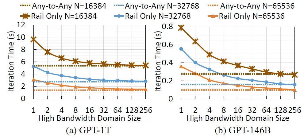
For a GPT-1T model, the performance gains are still quite significant when K>36 compared to K=8, but the marginal benefits of scaling from K>72 to K=576 do not justify the increased system complexity. Additionally, as the Scale-Up NVLINK network size grows, the performance benefits of the RDMA bandwidth between HBDs start to diminish. The ultimate balance is to use NVL72 combined with RDMA Scale-Out to construct a 32,000-card cluster.
Evolution of Interconnect Systems: The Story of Cisco
Distributed Architecture Due to Compute/Memory Bottleneck
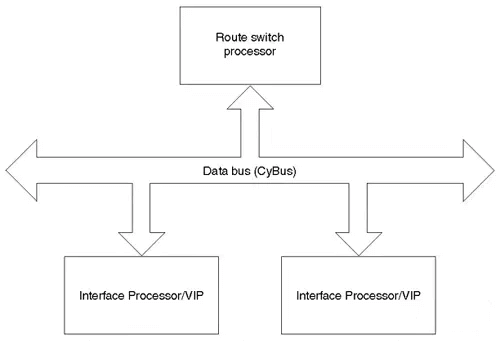
In the early days, Cisco’s routers used a single PowerPC processor to perform forwarding. As the internet exploded, the performance bottleneck was caused by memory-intensive operations like routing table lookups. This led to the gradual emergence of approaches like process switching/CEF, which connected multiple processors via a data bus:
These methods are similar to early NVLINK 1.0 / NVLINK 2.0, where chips were directly interconnected via a bus, like the Pascal generation.
The Emergence of Switch Fabric
In 1995, Nick Mckeown proposed using a CrossBar switch fabric to support higher-scale Gigabit routers in his paper “Fast Switched Backplane for a Gigabit Switched Router” – which later became Cisco’s high-end 12000 series routers.
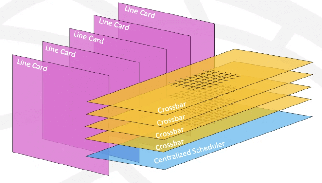
The switch fabrics in these systems are conceptually identical to today’s NVSwitch and NVSwitch Tray that build NVL8~NVL72 systems. They are all about interconnecting multiple chips to build a larger-scale system when a single chip hits the memory wall.
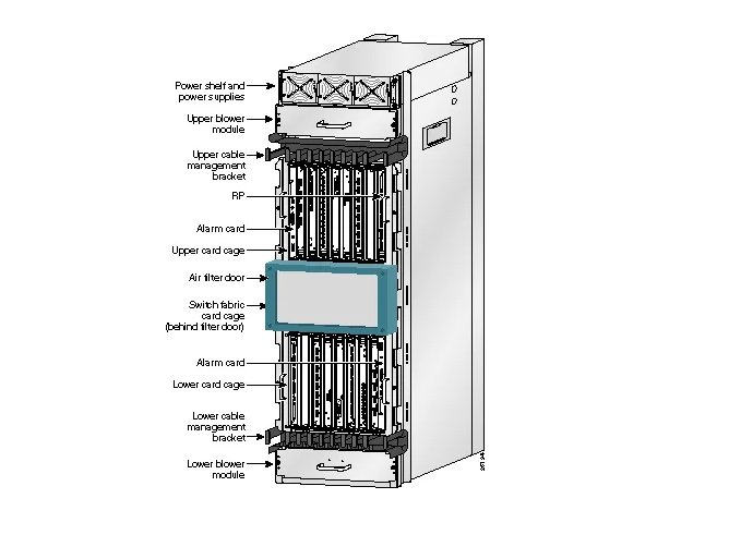
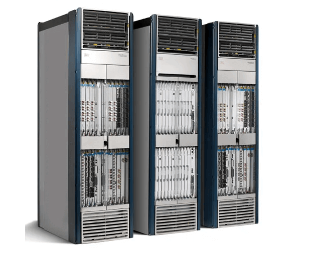
The single-chassis design of Cisco 12000, with the Switch Fabric in the middle and 9 Switch Trays, is similar to the GB200, where the top and bottom have 8 line card slots each, corresponding to the Compute Trays in GB200.
The core technology here is the VOQ (Virtual Output Queuing) design and iSLIP scheduling algorithm. When the model executes All-to-All, multiple B200s may write to the same B200 simultaneously, causing Head-Of-Line Blocking (HOLB). Humans cleverly add buffers before and after intersections, which are the Input Queue and Output Queue:
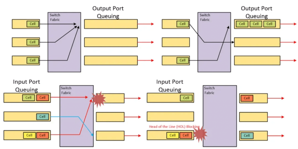
Unfortunately, the Output Queue can maximize bandwidth utilization but requires N*R speed, while the Input Queue can process at R speed but suffers from HOLB. The maximum throughput of an IQ switch limited by HOLB is calculated to be 58.6%.
A simple solution to the IQ HOLB problem is to use Virtual Output Queue (VOQ), where each input port has a queue for each output, eliminating HOLB while maintaining R-speed buffering.
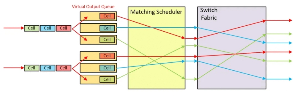
Of course, NVIDIA’s NVLINK uses a credit-based design, and credit distribution arbitration is an area worth in-depth research for domestic GPU startups.
Multi-Stage Architecture and the Evolution of Optical Interconnects
The NVL576 is similar to Cisco’s Carrier Routing System (CRS-1) introduced in 2003.
At that time, Cisco built a multi-stage switching network system facing the huge bandwidth demand during the internet bubble.
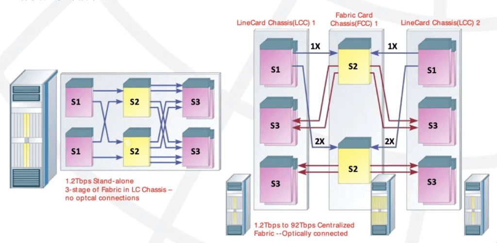
The 3-stage switching network within a single cabinet, constructed using Switch Trays, is equivalent to the current non-scalable GB200 NVL72. The multi-cabinet structure then corresponds to NVL576. Back then, Cisco could expand from a single cabinet with 16 Line Cards to a system with 8 Fabric cabinets + 72 Line Card cabinets, building a large-scale 1152 Line Card cluster. Cisco’s internal connections also use optical interconnects.
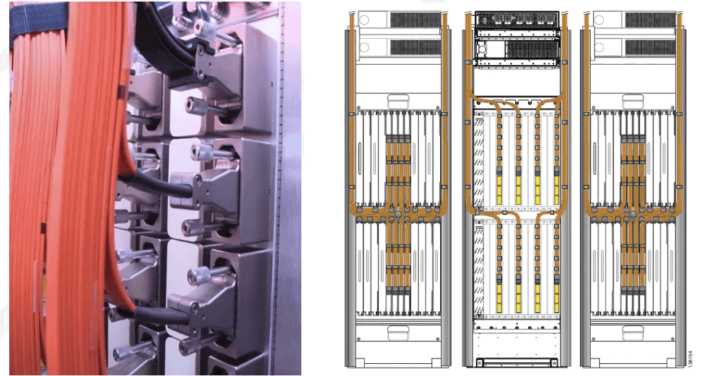
The inter-chassis optical connectors are shown in the image.
It’s worth noting that during this time, Bill Dally, now NVIDIA’s Chief Scientist, founded Avici and used 3D-Torus interconnects to build Terabit-scale routers.
The 3D-Torus interconnect reminds one of Google’s TPU. Later, Huawei OEM’d Avici’s system and branded it as NE5000, before developing their core router product NE5000E. Concurrently, the emergence of Juniper also put significant pressure on Cisco in the core router domain. Perhaps NVIDIA’s dominance will also face more challenges going forward.
On the other hand, MEMS-based optical switches were also introduced around that era, which seems to have some similarities to Google’s current use of optical switches.
NVIDIA’s Future Evolution
At the 2023 HOTI conference on interconnect systems, Bill Dally gave a keynote titled “Accelerator Clusters, The New Supercomputer”, discussing three main topics from the perspective of on-chip networks and interconnect systems:
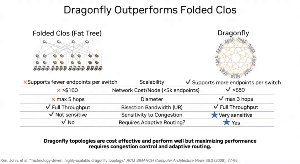
Topology:
- CLOS/3D-Torus/Dragonfly
- Routing:
- Flow control
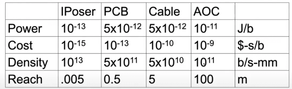
Different device connections have varying bandwidths and power consumption.
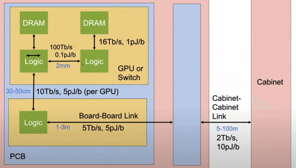
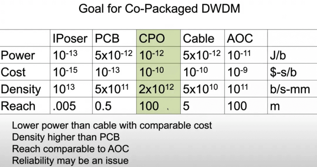
The challenge is how to organically combine them, considering factors like power, cost, density, and connection distance.
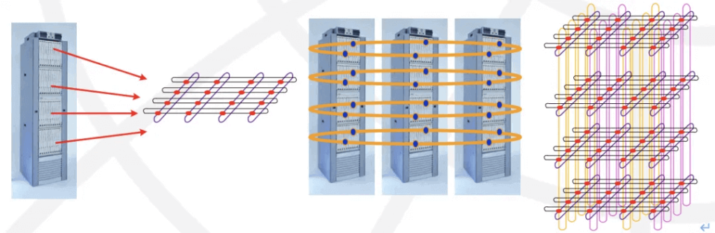
Optical Interconnects
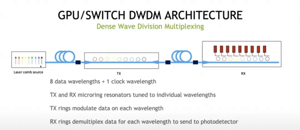
Through these dimensional measurements, Co-Package Optic DWDM becomes a viable choice:
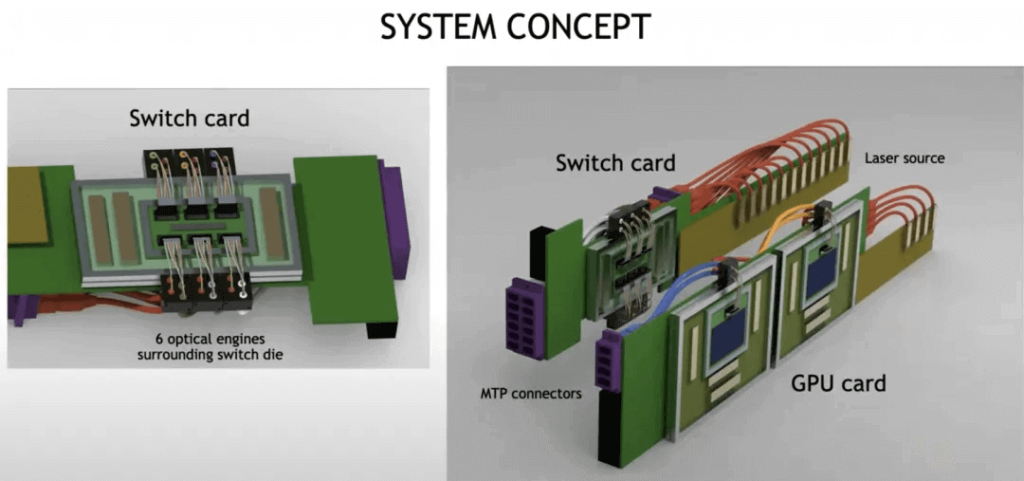
The system concept diagram for building optical interconnects is as follows:
The ultimate goal is to construct a massive-scale optical interconnect system.
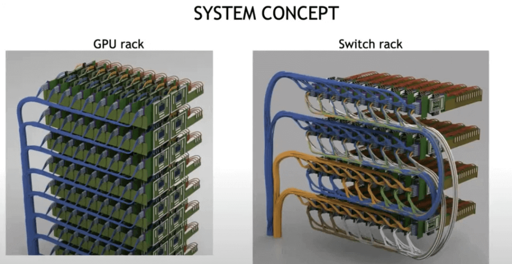
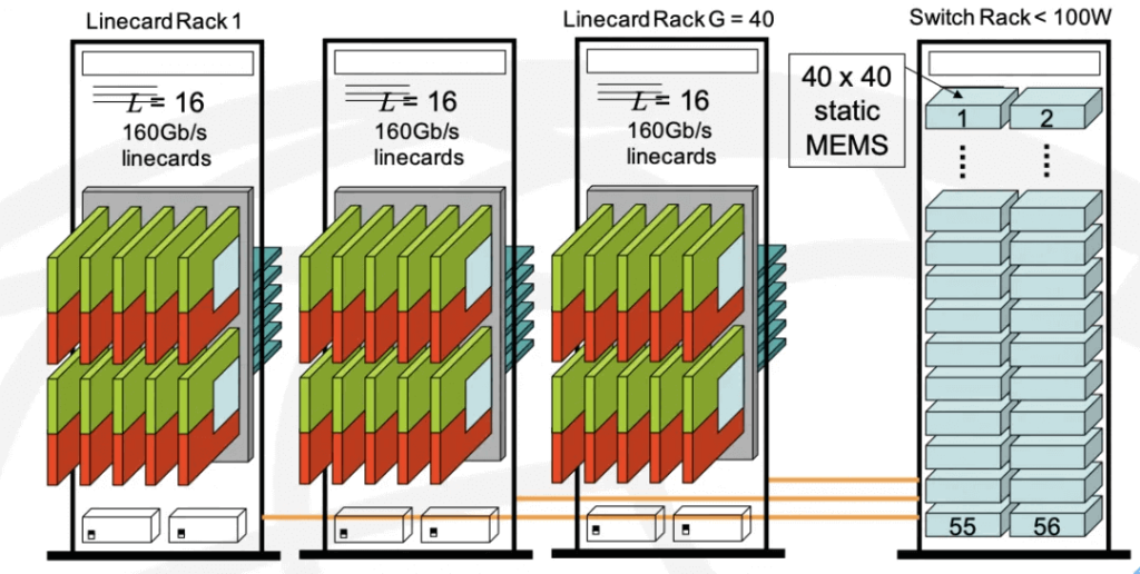
In this aspect, you will see that it is almost identical to the multi-chassis CRS-1 system that Cisco built, where the GPU Rack is equivalent to the Cisco LineCard Chassis, and the Switch Rack is equivalent to Cisco’s Fabric Chassis. They both use optical interconnects and DWDM technology to reduce connection complexity and increase bandwidth.
At the chip architecture level, an Optical Engine is used as a chiplet for interconnection.
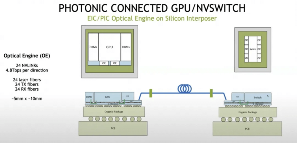
For the interconnect structure, there is a greater inclination towards adopting the Dragonfly topology and utilizing OCS optical switches.
As for flow control algorithms and congestion control, Bill discussed mechanisms similar to HOMA/NDP and Adaptive Routing. It is not necessary to be that complex, as we have better MultiPath CC algorithms that do not require any new switch features.
Algorithms and Special Hardware Integration
On the other hand, Transformer has been around for 7 years, and it is an excellent algorithm that balances compute-bound and memory-bound operators. However, is there an even more sophisticated algorithm in the industry?
Sparse Attention models like Monarch Mixer, and models that do not require Attention like Mamba/RMKV, as well as algorithms based on category theory, algebraic geometry, and algebraic topology, are being researched. There are also different numerical formats like FP4/FP6 supported by Blackwell, and potentially Log8 in the future.
Historically, Cisco also relied on algorithms and special hardware to gradually improve single-chip performance and overcome the complexity of interconnect structures. They used algorithms like TreeBitMap for large-scale routing table lookups on regular DRAM.
With the development of multi-core and on-chip networks, they built high-performance SPP/QFP/QFA network processors, and these technologies have resurfaced in AWS Nitro, NVIDIA BlueField, and Intel IPU DPU processors.
Conclusion
FibeMall analyzed the latest Blackwell GPU’s interconnect architecture and explored the distributed system construction and interconnect architecture that Cisco and NVIDIA faced when single-chip performance could not keep up with the explosive demand during two technology waves, as discussed in “NVIDIA’s Cisco Moment”. It also analyzed Bill Dally’s 2023 HOTI keynote, providing a clear view of NVIDIA’s future development path.
However, we also note that during the internet bubble peak, companies like Juniper and Avici emerged as challengers to Cisco, and NVIDIA also defeated 3Dfx as a challenger in that era before dominating the professional market. Every era has its opportunities, and the winners are not simply those who pile on more resources, but those who innovate through the combination of algorithms and computing power with hardware.
From the challenger’s perspective, the difficulty of the computing core itself, apart from the CUDA ecosystem, is not that great. Recently, Jim Keller and some HBM players in South Korea and Japan have been active, and whether BUDA+RISC-V+HBM will become a new emerging force is worth watching.
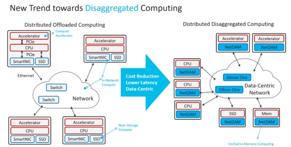
From the perspective of replacing IB/NVLINK interconnect systems, Ethernet already has 51.2Tbps switch chips, and communication protocols based on high-speed Ethernet connections to HBM, supporting in-network computing like SHARP, were already designed in NetDAM three years ago.
Related Products:
-
 OSFP-800G-FR4 800G OSFP FR4 (200G per line) PAM4 CWDM Duplex LC 2km SMF Optical Transceiver Module
$3500.00
OSFP-800G-FR4 800G OSFP FR4 (200G per line) PAM4 CWDM Duplex LC 2km SMF Optical Transceiver Module
$3500.00
-
OSFP-800G-2FR2L 800G OSFP 2FR2 (200G per line) PAM4 1291/1311nm 2km DOM Duplex LC SMF Optical Transceiver Module
$3000.00
-
OSFP-800G-2FR2 800G OSFP 2FR2 (200G per line) PAM4 1291/1311nm 2km DOM Dual CS SMF Optical Transceiver Module
$3000.00
-
OSFP-800G-DR4 800G OSFP DR4 (200G per line) PAM4 1311nm MPO-12 500m SMF DDM Optical Transceiver Module
$3000.00
-
NVIDIA MMS4X00-NM-FLT Compatible 800G Twin-port OSFP 2x400G Flat Top PAM4 1310nm 500m DOM Dual MTP/MPO-12 SMF Optical Transceiver Module
$1199.00
-
NVIDIA MMA4Z00-NS-FLT Compatible 800Gb/s Twin-port OSFP 2x400G SR8 PAM4 850nm 100m DOM Dual MPO-12 MMF Optical Transceiver Module
$650.00
-
NVIDIA MMS4X00-NM Compatible 800Gb/s Twin-port OSFP 2x400G PAM4 1310nm 500m DOM Dual MTP/MPO-12 SMF Optical Transceiver Module
$900.00
-
NVIDIA MMA4Z00-NS Compatible 800Gb/s Twin-port OSFP 2x400G SR8 PAM4 850nm 100m DOM Dual MPO-12 MMF Optical Transceiver Module
$650.00
-
NVIDIA MMS1Z00-NS400 Compatible 400G NDR QSFP112 DR4 PAM4 1310nm 500m MPO-12 with FEC Optical Transceiver Module
$850.00
-
NVIDIA MMS4X00-NS400 Compatible 400G OSFP DR4 Flat Top PAM4 1310nm MTP/MPO-12 500m SMF FEC Optical Transceiver Module
$700.00
-
NVIDIA MMS4X50-NM Compatible OSFP 2x400G FR4 PAM4 1310nm 2km DOM Dual Duplex LC SMF Optical Transceiver Module
$1200.00
-
OSFP-XD-1.6T-4FR2 1.6T OSFP-XD 4xFR2 PAM4 1291/1311nm 2km SN SMF Optical Transceiver Module
$15000.00
-
OSFP-XD-1.6T-2FR4 1.6T OSFP-XD 2xFR4 PAM4 2x CWDM4 2km Dual Duplex LC SMF Optical Transceiver Module
$20000.00
-
OSFP-XD-1.6T-DR8 1.6T OSFP-XD DR8 PAM4 1311nm 2km MPO-16 SMF Optical Transceiver Module
$12000.00