In the rapidly evolving world of data communication and high-performance computing, silicon photonics optical modules are emerging as a groundbreaking technology. Combining the maturity of silicon semiconductor processes with advanced photonics, these modules promise higher speeds, lower power consumption, and reduced costs. This in-depth guide explores the fundamentals, principles, advantages, industry landscape, challenges, and future trends of silicon photonics.
Part 01: Basic Concepts of Silicon Photonics
1. Definition of Silicon Photonics
Silicon photonics, also known as silicon-based optoelectronics, refers to the integration of multiple optical devices on a single silicon substrate. More simply, while traditional semiconductors like CPUs, GPUs, and SoCs in computers and smartphones are silicon-based integrated circuits, silicon photonics merges silicon semiconductor manufacturing with optical communication technologies. It enables the fabrication and integration of optical devices directly on silicon wafers, facilitating the transmission and processing of optical signals through photonic integrated circuits (PICs).
In essence: Silicon Photonics = CMOS Technology (ultra-large-scale logic and ultra-high-precision manufacturing) + Photonics Technology (ultra-high speed and ultra-low power consumption). This approach integrates numerous discrete optical and electrical components into a single microchip, achieving high integration, low power consumption, and low cost.
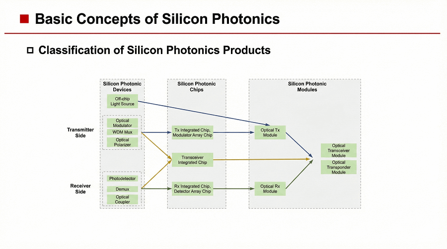
2. Classification of Silicon Photonics Products
Strictly speaking, silicon photonics technology encompasses three levels:
- Silicon Photonics Devices: Fundamental components, including lasers, modulators, detectors, planar waveguides, and grating couplers.
- Silicon Photonics Chips: Integrated assemblies of various silicon photonics devices.
- Silicon Photonics Modules: The product form of silicon photonics technology, integrating light sources, silicon photonics chips, modules, and external driver circuits into a unified package.
3. Forms of Silicon Photonics
- Monolithic Integration: All optical components (including light sources, modulators, waveguides, and couplers) are fabricated directly on the same silicon chip, forming a compact optical circuit. Advantages: Reduced size, higher integration density, and lower manufacturing costs.
- Hybrid Integration: Combines silicon chips with optical components made from other materials, integrating electronic devices (e.g., SiGe, CMOS, RF) and photonic devices (e.g., lasers/detectors, optical switches, modulators) on a silicon substrate. The silicon chip primarily handles electronic processing, while other materials manage light generation and modulation. Advantages: Leverages the strengths of silicon electronics and superior optical properties of alternative materials.
4. Technical Advantages of Silicon Photonics
- High Integration Density: Silicon’s high refractive index and strong optical confinement enable narrower waveguides and smaller bending radii, significantly boosting integration density.
- High Speed: With a bandgap of 1.12 eV (corresponding to 1.1 μm wavelength), silicon is nearly transparent and low-loss in the 1.1–1.6 μm communication bands (typical wavelengths: 1.31 μm and 1.55 μm).
- Low Cost: Silicon is the second most abundant element on Earth, with low material costs and support for large-wafer manufacturing. Production leverages mature CMOS processes, enabling mass production and substantial cost reduction potential.
- Interference Resistance: Optical signals are immune to electromagnetic noise, enhancing reliability.
- Low Power Consumption: Optical transmission eliminates resistive losses, improving energy efficiency by approximately 10x compared to electrical signals.
5. Silicon Photonics vs. Traditional Electrical Interconnects
Silicon photonics outperforms traditional electrical interconnects in bandwidth, latency, and power efficiency, making it ideal for data centers and AI-driven infrastructures.
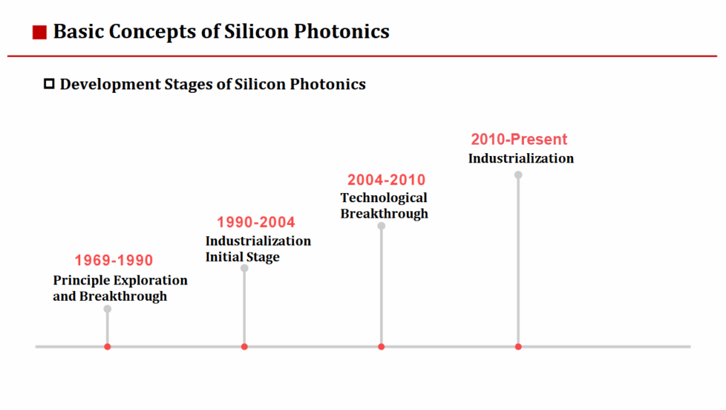
6. Development History of Silicon Photonics
- 1969: S.E. Miller at Bell Labs proposed the concept of integrated optics (limited commercialization due to technological constraints).
- 1985: Richard Soref discovered the plasma dispersion effect in crystalline silicon, providing a theoretical foundation for silicon-based electro-optic modulation.
- 1991: The U.S. established the Optoelectronic Industry Development Association to attract investment.
- 2004: Intel developed the first silicon-based modulator using MOS capacitors, achieving >1 GHz bandwidth.
- 2005: Intel demonstrated the world’s first continuous-wave all-silicon laser using the Raman effect.
- 2006: University of California and Intel jointly developed an electrically pumped III-V hybrid integrated laser.
- 2010: Intel released the first 50 Gb/s short-reach silicon integrated transceiver chip, marking the start of industrialization. Luxtera launched the first commercial silicon photonics module for 40 Gbps data center transmission.
- 2013: Luxtera introduced the first commercial 100G silicon photonics module.
- 2016: Cisco acquired silicon photonics company Acacia for $6.8 billion, shaking the industry.
Part 02: Silicon Photonics Optical Modules
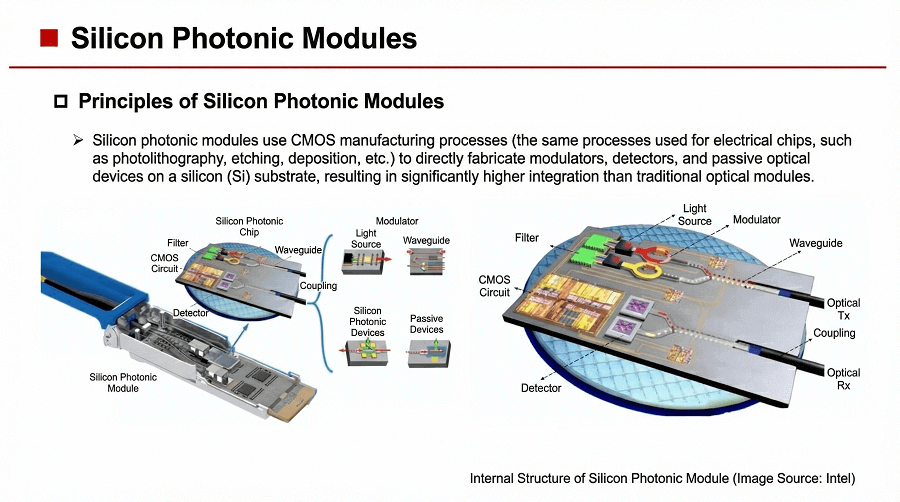
1. Principle of Silicon Photonics Optical Modules
These modules employ CMOS manufacturing processes (e.g., lithography, etching, deposition) to fabricate modulators, detectors, and passive optical devices directly on silicon substrates, achieving significantly higher integration than traditional optical modules.
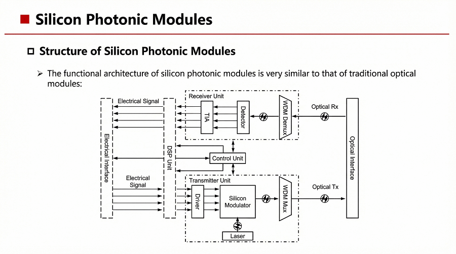
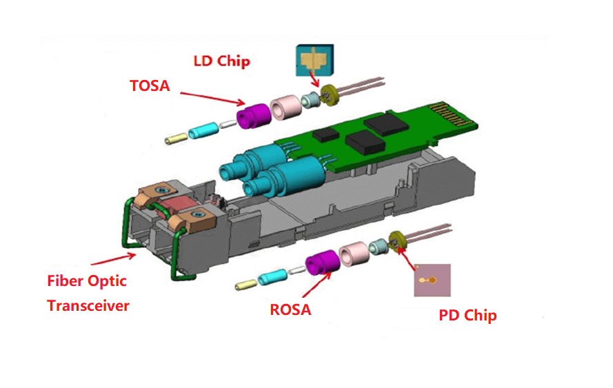
2. Structure of Silicon Photonics Optical Modules
The functional architecture mirrors traditional optical modules, with core components including:
- Transmitter Optical Sub-Assembly (TOSA): Converts electrical signals to optical signals.
- Receiver Optical Sub-Assembly (ROSA): Converts optical signals to electrical signals.
- Silicon Photonics Chip: Integrates waveguides, modulators, detectors, etc.
- Peripheral Circuits: Driver ICs, transimpedance amplifiers (TIAs), and more.
3. Key Devices in Silicon Photonics Modules
Devices are categorized as active or passive:
(1) Lasers
- Principle: Uses semiconductor materials as gain media, converting injected electrical energy into laser output via optical resonance.
- Types:
- VCSEL (Vertical-Cavity Surface-Emitting Laser): Emits light perpendicular to the chip; suited for short distances (<200 m).
- EEL (Edge-Emitting Laser): Emits light parallel to the substrate; used for medium-to-long distances. Subtypes include FP, DFB (directly modulated lasers, DML), and EML (electro-absorption modulated lasers integrated with DFB for high-speed, long-distance transmission).
- Challenge: Silicon is an indirect bandgap semiconductor and cannot emit light efficiently. Thus, III-V materials (e.g., GaAs, InP) lasers are externally integrated.
(2) Modulators
- Function: Modulates light to increase bandwidth and support higher speeds.
- Principle: Plasma dispersion effect—voltage changes carrier concentration, altering refractive index and controlling light intensity or phase.
- Common Types: Mach-Zehnder Modulator (MZM) and Micro-Ring Resonator (MRR).
(3) Detectors
- Function: Converts optical signals to electrical via the photoelectric effect.
- Materials: Typically germanium (Ge) integrated with silicon waveguides.
- Types: PIN diodes (medium sensitivity, short-to-medium distance) and APD (avalanche photodiodes, higher sensitivity for longer distances).
(4) Waveguides
- Function: Guides light propagation via total internal reflection in micron-scale channels, exploiting refractive index differences between silicon and silicon dioxide.
(5) Multiplexers and Demultiplexers
- Function: Enable multi-wavelength parallel transmission for higher bandwidth.
- Types: Arrayed Waveguide Gratings (AWG), Micro-Ring Resonators (MRR), and cascaded Mach-Zehnder Interferometers (MZI).
(6) Optical Coupling
- Challenge: Precise alignment between nanoscale waveguides and fibers; minor misalignment causes significant insertion loss.
- Methods: Edge coupling (low loss, wide bandwidth, high process difficulty) and grating coupling (larger alignment tolerance, suitable for wafer-level testing, but higher loss and polarization/wavelength sensitivity).
4. Advantages of Silicon Photonics Optical Modules
- High Integration: Reduces component count and volume by ~30%, increasing port density.
- Low Cost: Leverages affordable silicon substrates and mature CMOS supply chains.
- Low Power Consumption: Reduced connection losses and often no need for TEC; ~40% lower than traditional modules.
- Mature Supply Chain: Benefits from semiconductor technology with low dependence on advanced nodes (hundreds of nm sufficient).
Part 03: Silicon Photonics Industry Chain
1. Key Industry Players
The ecosystem features diverse participants: vertically integrated leaders (e.g., Innolight, Cisco), startups (e.g., Xphor, DustPhotonics), research institutions (e.g., UCSB, Columbia University), foundries (e.g., Tower Semiconductor, TSMC), and equipment suppliers (e.g., Applied Materials, ASML). Notable companies: Intel, Cisco, GlobalFoundries, Coherent, Lumentum, Broadcom.
2. Application Scenarios
- Optical Communication: Driven by AI computing, 800G/1.6T modules are mainstream; silicon photonics is key for ultra-high-speed scenarios. Market projected to exceed $6 billion by 2025.
- LiDAR: Enables low-cost, compact solid-state systems for autonomous driving and industrial automation.
- Optical Computing: Harnesses parallel processing and low latency for AI accelerators with exceptional energy efficiency.
- Quantum Communication: Provides highly integrated optical control for entangled photon manipulation.
- Biosensing: High-sensitivity chip-scale sensors for portable medical diagnostics and environmental monitoring.
3. Optical Chip Manufacturing Process (Laser Example)
- Chip design.
- Epitaxial growth (MOCVD/MBE).
- Wafer fabrication (gratings, waveguides, lithography, etching).
- Chip processing and testing (cleaving, coating, packaging, reliability testing).
Part 04: Challenges Facing Silicon Photonics
1. Core Material and Integration Bottlenecks
- Silicon cannot produce efficient on-chip light sources.
- Heterogeneous integration of III-V lasers is complex due to lattice mismatch and thermal expansion differences.
- Extremely tight process tolerances.
2. Design, Manufacturing, and Packaging Difficulties
- Immature EPDA tools compared to EDA.
- Yield challenges critical for mass production (e.g., ~65% in CPO packaging).
- High packaging costs (~90% of total) due to precise optical alignment.
3. Industrialization and Ecosystem Challenges
- High initial R&D costs; advantages emerge only at scale.
- Lack of standardized ecosystem; gaps in domestic EPDA tools and platforms.
- Limited cost-effectiveness in long-haul telecom or low-speed scenarios; maintainability issues in emerging tech like CPO.
4. Future Trends in Silicon Photonics
Despite hurdles, silicon photonics is rapidly becoming essential infrastructure for the computing era. Advances in materials, integration processes, yield improvement, and open ecosystems will drive penetration across communication, computing, and sensing—positioning it as a core pillar of future information technology.
For professionals exploring next-generation optical solutions, silicon photonics optical modules represent a transformative opportunity in high-speed, efficient data transmission. Stay updated as this technology continues to reshape the industry.
Related Products:
-
 OSFP-800G-FR8L OSFP 800G FR8 PAM4 CWDM8 Duplex LC 2km SMF Optical Transceiver Module
$3000.00
OSFP-800G-FR8L OSFP 800G FR8 PAM4 CWDM8 Duplex LC 2km SMF Optical Transceiver Module
$3000.00
-
OSFP-800G-LR8 OSFP 8x100G LR PAM4 1310nm MPO-16 10km SMF Optical Transceiver Module
$1800.00
-
OSFP-800G-FR8D OSFP 8x100G FR PAM4 1310nm Dual MPO-12 2km SMF Optical Transceiver Module
$1100.00
-
OSFP-800G-FR8 OSFP 8x100G FR PAM4 1310nm MPO-16 2km SMF Optical Transceiver Module
$1200.00
-
OSFP-800G-DR8 OSFP 8x100G DR PAM4 1310nm MPO-16 500m SMF DDM Optical Transceiver Module
$900.00
-
QSFP-DD-800G-FR8L QSFP-DD 800G FR8 PAM4 CWDM8 2km DOM Duplex LC SMF Optical Transceiver Module
$3000.00
-
OSFP-800G-SR8 OSFP 8x100G SR8 PAM4 850nm MTP/MPO-16 100m OM4 MMF FEC Optical Transceiver Module
$650.00
-
OSFP-800G-SR8D OSFP 8x100G SR8 PAM4 850nm 100m DOM Dual MPO-12 MMF Optical Transceiver Module
$650.00