With the commercialization of new IoT technologies such as cloud computing and big data and the gradual implementation of the 5th Generation Mobile Communication (5G) construction, the traffic transmitted in data centers is growing exponentially.
According to FiberMall’s research, the total number of major hyperscale data centers worldwide has grown to nearly 600 by the end of 2020, double what it was five years ago. With the increase in the number of data centers, the digital optical mode market also ushered in development opportunities. According to the statistics of well-known research institutions, the optical modules used in data centers reached 50 million in 2019, and the market value of optical modules in data centers is expected to exceed 4.9 billion dollars by the end of 2021. The rate of the original 100G optical module cannot meet the requirements of the current application scenarios. Therefore, it is imperative to improve the rate of the optical module to meet the transmission requirements. The 400 Gbit/s Quad Small Form Factor Pluggable-Double Density Short Range 8 optical module(400G QSFP-DD SR8), which meets the IEEE 802.3cm protocol, will become the mainstream optical module in data center with the advantages of high speed, low power consumption, low cost, and small size.
FiberMall proposes the optical path design of 400G QSFP-DD SR8 optical modules based on Chip on Board COB (COB) technology. It adopted integrated lens, designed the optical path, and carried out simulation optimization. According to Fresnel reflection, the contact Angle was increased to reduce the reflection. After selecting the appropriate inclined plane and determining the scheme, the receiving end and the originating end of the module are tested respectively to verify the feasibility of the optical path design.
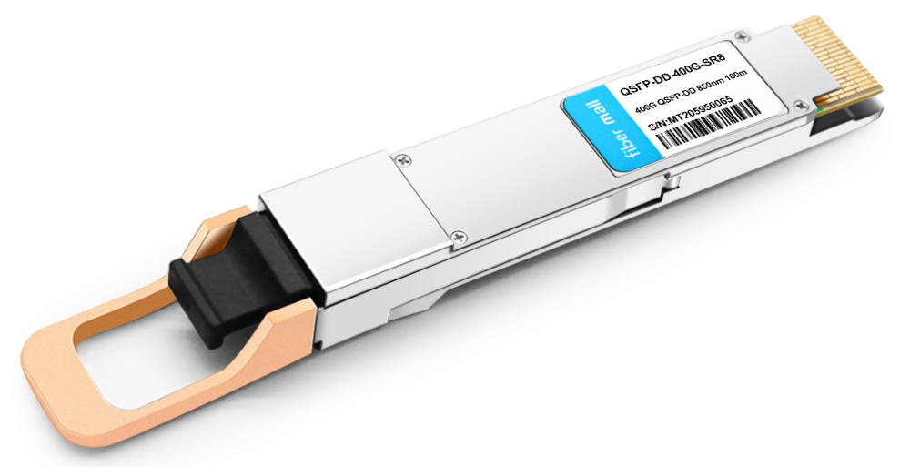
Figure 1. 400G QSFP-DD SR8
400G QSFP-DD SR8 Optical Path Design and Simulation
Vertical Cavity Surface Emitting Laser (VCSEL) is chosen as the light source for short-distance transmission in data centers. In order to meet the module packaging protocol standards, the optical path needs to be turned so that the vertical light from the VCSEL can enter the fiber in parallel. The module is required to stabilize the output power, which requires real-time monitoring of the working state of the VCSEL, adding a splitter to reflect part of the light emitted from the VCSEL to the Monitor Photo Diode (MPD) for backlight detection and control to stabilize the output power, and obtaining the overall light path architecture. The VCSEL is used as the light source at the transmitter, and it is necessary to convert the vertical light into parallel light coupling into the optical fiber for transmission. First, the light emitted by VCSEL is collimated and entered into the lens. After total reflection through the 45° surface, the vertically emitted beam is incident horizontally into the optical fiber after turning.
Since the VCSEL needs to be monitored, the thickness of the splitter needs to be considered to affect the optical path by controlling the tilt angle of the splitter to adjust the position of the MPD and changing the transmittance of the reflective film on the splitter to adjust the optical power range. The initial object distance relationship is obtained from the mechanical space, and the set object distance is 0.34 mm and the phase distance is 0.45 mm. Figure 2 shows the schematic diagram of the optical path at the transmitter.
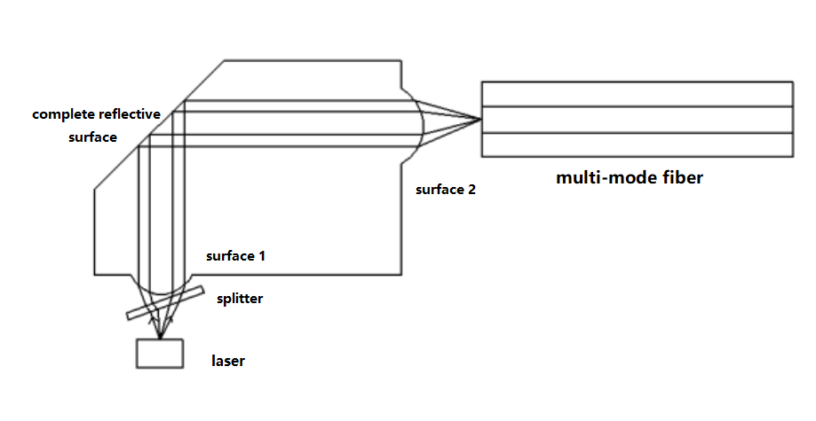
Figure 2. The schematic diagram of the optical path at the transmitter
The receiving end is similar to the transmitting end, where the PD receives the horizontal incident light from the fiber, first passes through the spherical collimation of the fiber end lens, turns the incident beam through a 45° total reflection surface, then passes through the lens to collimate the beam, and finally is received by the PD.
Since the integrated lens is used, the design process needs to ensure the same object distance between the receiving end and the transmitting end. The objective distance at the receiving end is 0.23 mm and the image distance at the transmitting end is 0.45 mm. Figure 3 shows the optical path at the receiving end.
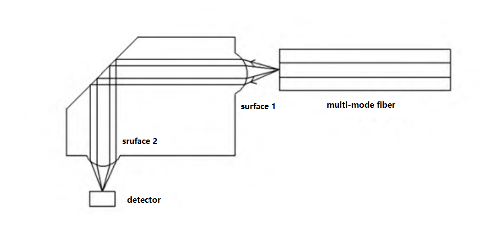
Figure 3. The optical path at the receiving end
400G QSFP-DD SR8 optical path simulation and optimization
The main parameters of the receiver and the transmitter are shown in Table 1.
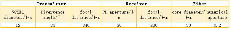
Table 1. Main parameters of the optical system
The object image relation and optical path structure in Table 1 were selected to design and simulate the lens coupling optical path by using ZEMAX software. The optimization function was used to adjust the surface shape of the two spheres to optimize the coupling efficiency, and then the contact Angle of the fiber was changed and different angles were set for simulation. Figure 4 shows the optical simulation of the TX end of the lens coupling system.
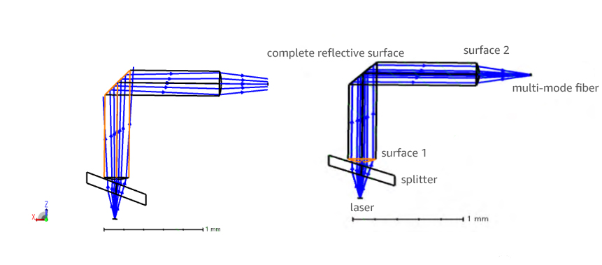
Figure 4. Optical simulation diagram
It can be found from the simulation that the degree of spot convergence before and after optimization is very different. Before optimization, some light has been lost, and the light spots received on the optical fiber side are large. Much light is difficult to enter the optical fiber, and the coupling efficiency is very low. The optimized optical path can achieve optical path convergence and higher coupling efficiency. The design and simulation of the optical path are completed, and the practical application should be considered.
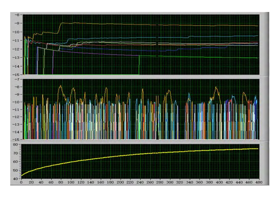
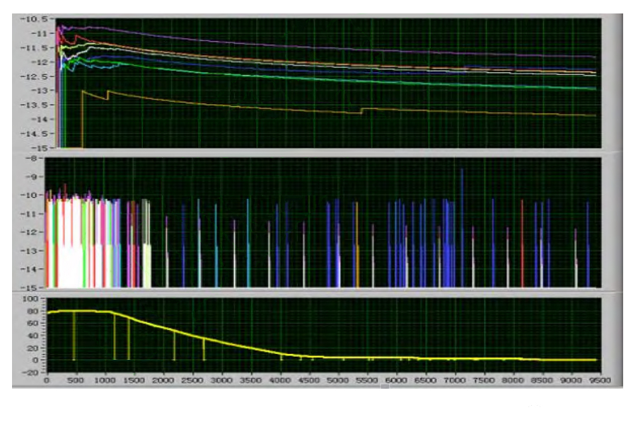
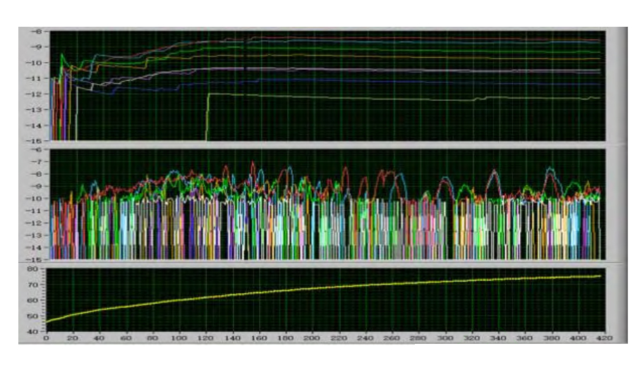
In manufacturing, due to the deviation of the process, the error of the VCSEL patch, the error of the production of lens optical port spacing, the deviation caused by the stress release of the glue in high-temperature curing, etc. These factors make it difficult for the actual coupling efficiency to reach the ideal situation, so it is necessary to carry out tolerance analysis to simulate the actual production situation. The tolerances in X, Y and Z axes after VCSEL offset are shown in figure 5. As can be seen from the figure, as long as the accuracy of the three directions is controlled within the range of ±9μm, the coupling efficiency is greater than 70%. However, considering the deviation in more than one direction may exist in the actual process, the patch error is controlled within ±3μm, so that the system has a high margin to prevent the decrease of coupling efficiency. In coupling the fiber into the lens we can see it as a whole. In practice, the coupling lens is followed by short fiber bonding. There may be good coupling but after loading staple fiber product performance is not up to standard. This is usually due to the mismatch between the size of the coupling fiber and the staple fiber or the location of the bond is not the location of the active coupling. Therefore, the tolerance of moving optical fiber is simulated by moving optical fiber. Figure 6 shows the change of the coupling efficiency of the mobile fiber. It can be seen from the figure that there are tolerances of 30μm in the X, Y and Z directions. The position of the moving lens directly reflects the tolerance range of the optical path design. Figure 7 shows the change in the coupling efficiency of the moving lens. As can be seen from the figure, it is necessary to select a motor with good consistency in the actual coupling of the product, otherwise too large deviation will easily lead to deviation between the actual position and the ideal optical path. In the process of optical module interconnection, the gap will inevitably occur when the two cores contact. At this time, the refractive index will change, and Fresnel reflection will occur at the joint. FIG. 8 shows the Fresnel reflection at the fiber optic junction. As can be seen from the figure, during the interconnection of optical modules, a Fresnel reflection will occur when the light from fiber 1 enters the air gap. Fresnel reflection is produced when it enters fiber 2 from the air gap. So whenever there is an air gap there will be two reflections. Due to the close distance between the connecting end and VCSEL, VCSEL will re-excite the reflected light and generate noise, resulting in burst error codes at the receiving end and affecting the module performance.
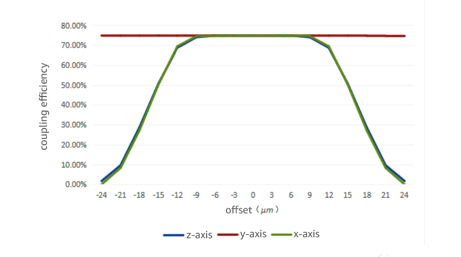
Figure 5. Changes in mobile VCSEL coupling efficiency
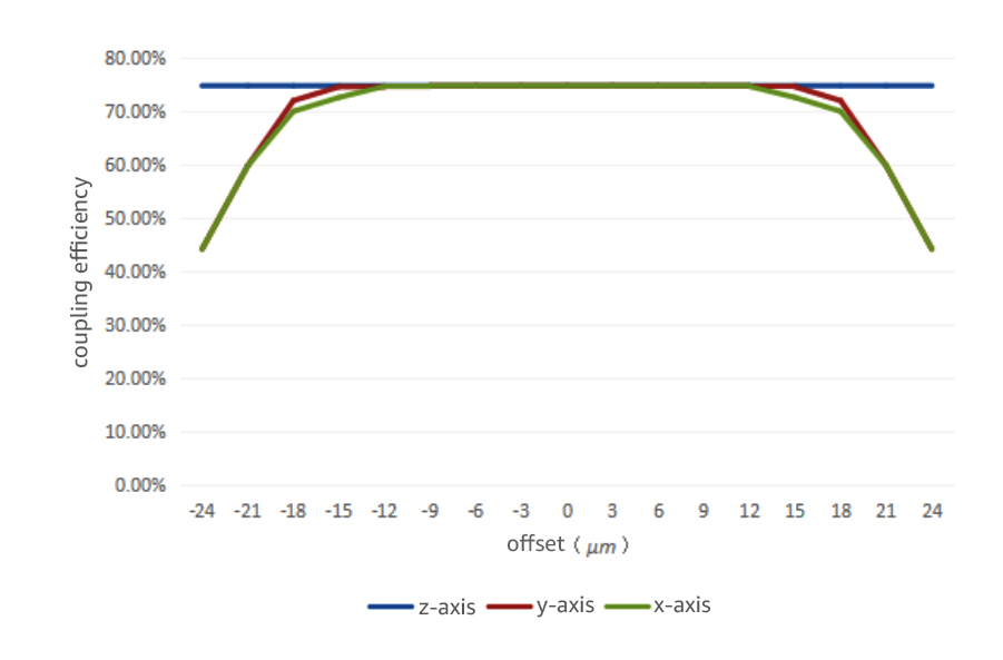
Figure 6. Change of coupling efficiency of mobile fiber
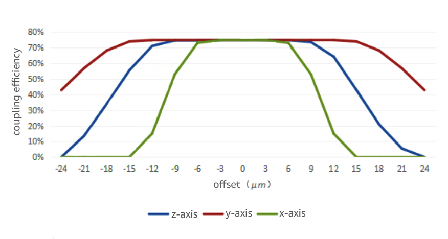
Figure 7. Change of coupling efficiency of moving lens

Figure 8. Fresnel reflection at the fiber joint. Note: n0 is the refractive index of air; n1 is the refractive index of the fiber core.
In this paper, the inclination Angle is increased on the contact surface of two optical fibers to change the direction of the reflected light so that it does not meet the requirements of total reflection and goes out of the cladding,and does not return to the Vcsel chip, so as to reduce the reflection of the module and improve the performance of the module. Through the simulation analysis of different inclination angles and the module test results, the final selection of the appropriate inclination.

Figure 9. Increase the Angle of the optical fiber connector
The reflection coefficients at different grinding angles can be obtained according to the Gaussian beam coupling theory.
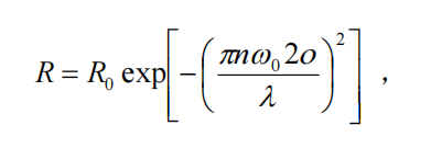
R0 is Fresnel reflection coefficient when plane; n is the refractive index of cladding; Ensure that the previous two are end Angle tilts. In practical use, it is also necessary to consider the optical power and the size of the annular luminous flux and select the appropriate tilt Angle.
Experimental Verification
A 400 Gbit/s QSFP-DD device was tested for annular light flux and receiver responsiveness to measure the change in product performance after changing the tilt Angle. Changing the tilt Angle will change the image distance of the optical path. Due to the different focal lengths, the receiver and the receiver will change the same image distance, and the object distance change is inconsistent, resulting in the change of the product’s optical path. In multi-mode optical communication systems, the Encircled Flux (EF) of VCSEL was used to define the optical characteristics of VCSEL emission and transmission. The responsivity is used to measure the photoelectric conversion performance of PD and the optical path performance at the receiving end. The coupling efficiency of the receiving end can be calculated through the responsivity tests. As shown in Table 2, the outgoing optical power, loop flux and receiver responsivity under different tilt angles are measured.
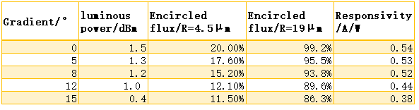
Table 2. Device testing at different angles
The service capability of the module is measured by testing the self-loop performance of the module at high temperatures. The reflected light will cause burst error of the module. The code type of the bit error detector was adjusted to PRBS31Q, and the receiving and sending of the module were connected through the self-loop fiber, so as to test the bit error caused by the temperature change. It can be seen from Table 2 that, except for the response at 15° and the deterioration of the encircled flux to the range, the rest are within the range (when R=4.5μm, EF < 30%; When R=19μm, EF≥86%), the encircled flux decrease at 4.5μm can effectively reduce the reflection. FIG. 10 shows the changes of the real-time bit error rate and total bit error rate of the test module with temperature. Different colors represent different channels respectively. As can be seen from figure 10 (a) and 10 (b), burst error will still occur when plane fiber connection and 5° connection are selected. As shown in figure 10 (d), the receiving performance has decreased when 12° connection is selected.
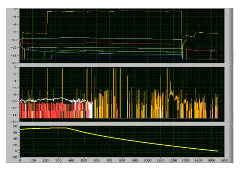
(a) Fiber testingat 0°
(b) Fiber testingat 5°
(c) Fiber testingat 8°
(d) Fiber testingat 12°
Figure 10. High-temperature fiber transfer test at different tilt angles
In the test of the 400G QSFP-DD module, the transmitter generates a 31-order signal source from the error code analyzer and connects to the optical module to be measured through 8 pairs of differential RF lines. The module eye test is shown in Figure 11, and the sensitivity of the receiving module is mainly tested. By changing the ambient temperature to test the working condition of the receiving and sending terminals of the module at three temperatures, the results are shown in Table 2-5.
Test the eye diagram of the module and the sensitivity, extinction ratio, Optical Modulation Amplitude (OMA), Transmitter and Dispersion Eye Closure Quaternary (TDECQ), and other tests under the three-temperature state to evaluate the optical path design effect.
From the test data, it is found that the module works stably at the third temperature, and the channel difference is small. All the modules are within the scope of the protocol and have a large margin.
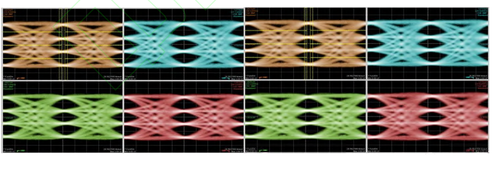
Figure 11. The module eye test
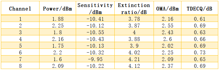
Table 3. Performance test results of optical module at room temperature
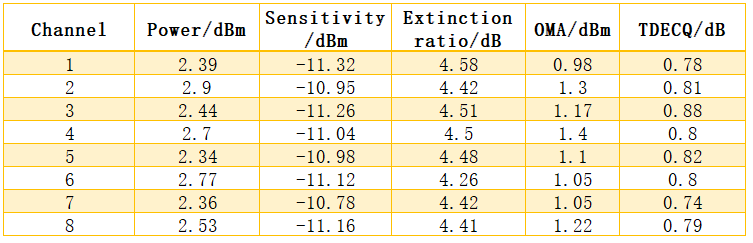
Table 4. Performance test results of optical module at low temperature
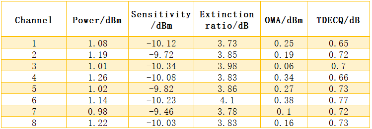
Table 5. Performance test results of optical module at high temperature
Conclusion
The COB design solution of 400G QSFP-DD SR8 optical transceivers is proposed in this paper. Through the optical path design and simulation, the tolerance width and coupling efficiency under three axes are obtained, and the coupling efficiency changes under different errors. It provides guidance for the production of the device and tests the performance and error of the device under different grinding angles. Finally, the 8° Angle was determined for adaptation, and the module test platform was built to verify that the design should be good. The performance of the test meets the IEEE 802.3cm protocol standard and meets the requirements of the design index. This design improves product performance and reduces optical reflection to a certain extent. It is the best choice for the next-generation data center.
Related Products:
-
 QSFP-DD-400G-SR8 400G QSFP-DD SR8 PAM4 850nm 100m MTP/MPO OM3 FEC Optical Transceiver Module
$149.00
QSFP-DD-400G-SR8 400G QSFP-DD SR8 PAM4 850nm 100m MTP/MPO OM3 FEC Optical Transceiver Module
$149.00
-
Cisco QDD-400G-SR8-S Compatible 400G QSFP-DD SR8 PAM4 850nm 100m OM4 MPO-16 DDM MMF Optical Transceiver Module
$149.00
-
Arista Networks QDD-400G-SR8 Compatible 400G QSFP-DD SR8 PAM4 850nm 100m MTP/MPO OM3 FEC Optical Transceiver Module
$149.00
-
DELL 400G-Q56DD-SR8 Compatible 400G QSFP-DD SR8 PAM4 850nm 100m MTP/MPO OM3 FEC Optical Transceiver Module
$149.00
-
EdgeCore ET7502-SR8 Compatible 400G QSFP-DD SR8 PAM4 850nm 100m OM4 MPO-16 DDM MMF Optical Transceiver Module
$149.00
-
H3C QSFPDD-400G-SR8-MM850 Compatible 400G QSFP-DD SR8 PAM4 850nm 100m MTP/MPO OM3 FEC Optical Transceiver Module
$149.00
-
NVIDIA(Mellanox) QMMA1U00-WS Compatible 400G QSFP-DD SR8 PAM4 850nm 100m MTP/MPO OM3 FEC Optical Transceiver Module
$149.00
-
NVIDIA T-DQ8FNS-N00-M Compatible 400G QSFP-DD SR8 PAM4 850nm 100m MTP/MPO OM3 FEC Optical Transceiver Module
$149.00