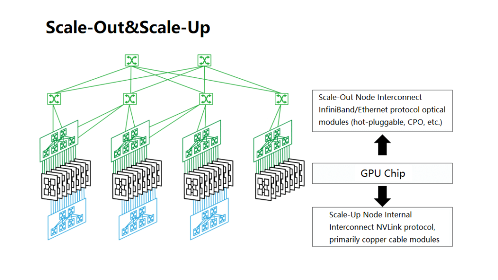
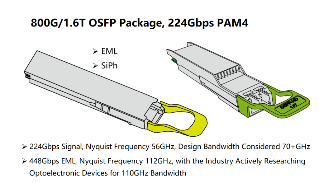
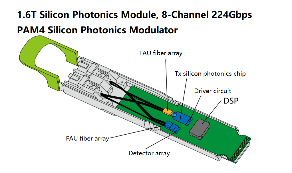
Artificial intelligence demands extraordinarily large computational power. In high-performance computing systems, there is a clear divergence in approach: scale-up systems rely on copper cable modules, while scale-out systems are increasingly dependent on optical modules. This year, detailed analyses have been conducted on copper cable modules used for scale-up applications. In contrast, optical modules dominate scale-out architectures. Traditional hot-pluggable optical modules are evolving from a single-lane configuration operating at 224 Gbps PAM4 toward systems supporting 800 G and 1.6 T rates.
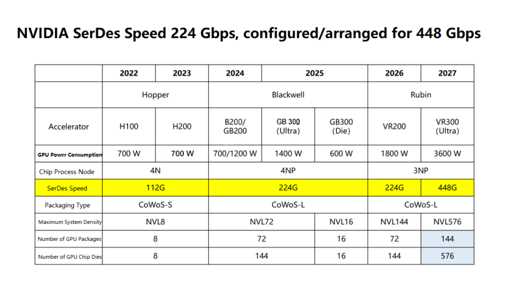
Meanwhile, Co-Packaged Optics (CPO) is emerging as an important development. In all these configurations—cable modules, traditional hot-pluggable optical modules, and CPO—the challenge is to advance from 112 Gbps PAM4 signal processing to optimized higher-speed processing at 224 Gbps PAM4. Major industry players are actively researching various optoelectronic chip and packaging technologies aimed at achieving 448 Gbps PAM4 performance.
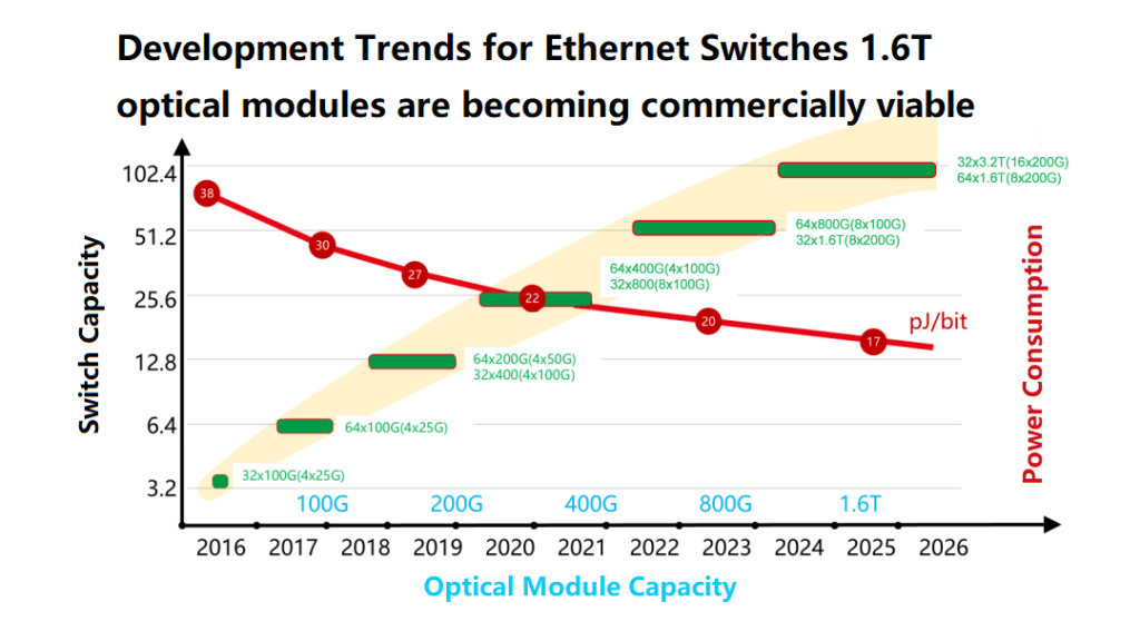
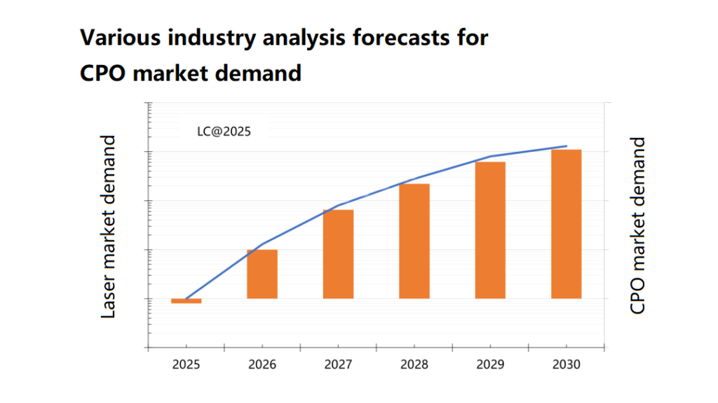
By 2025, early indications suggest that 1.6 T optical modules will begin to see commercial deployment, marking the transition of these technologies from laboratory research to industrial application.
It is important to note that a pure 200 Gbps PAM4 data signal, after encoding, effectively becomes either 212 Gbps PAM4 or 224 Gbps PAM4. Although the designations 200 Gbps PAM4, 212 Gbps PAM4, and 224 Gbps PAM4 might appear distinct in certain contexts, they essentially refer to the same underlying performance level.
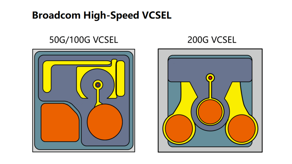
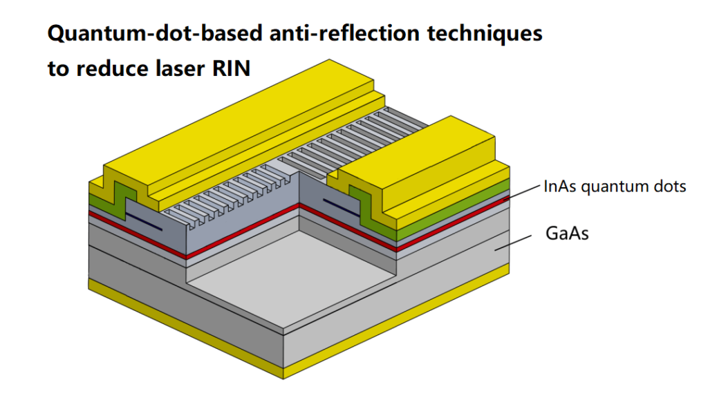
Within the industry, multimode systems typically employ Vertical-Cavity Surface-Emitting Lasers (VCSELs), while single-mode configurations are based on Electro-absorption Modulated Lasers (EML) or silicon photonics. An intrinsic conversion relationship exists between signal frequency bandwidth, bit rate, and baud rate. Notably, the bandwidth expansion achievable by VCSELs is slightly inferior to that of EML or silicon photonics. At present, the multimode VCSEL sector is deploying 100 Gbps PAM4 solutions while actively researching 200 Gbps PAM4, whereas EML and silicon photonics are already deployed at 200 Gbps PAM4 levels with ongoing investigations into extending capabilities to 400 Gbps PAM4.
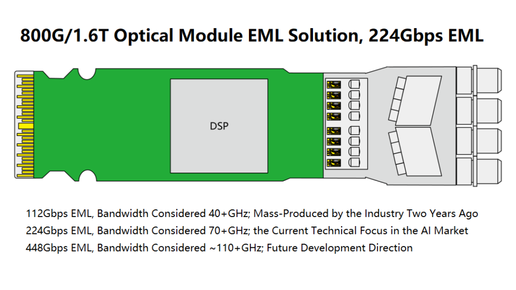
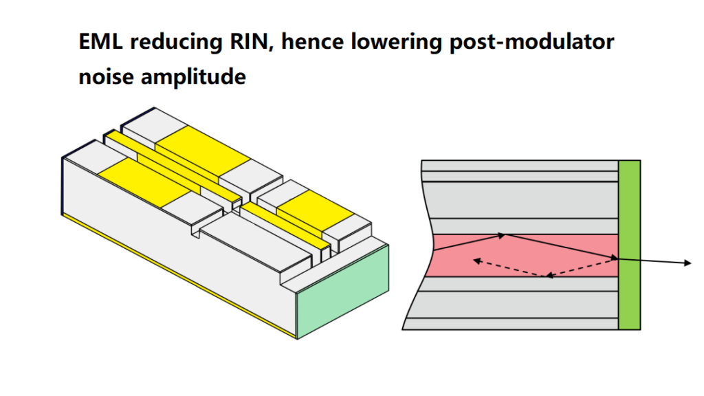
Companies such as Lumentum, Broadcom, Mitsubishi, and Huawei HiSilicon are pursuing developments in 224 Gbps EML technology as well as optoelectronic chips that can support speeds exceeding 300 G and even 400 Gbps.
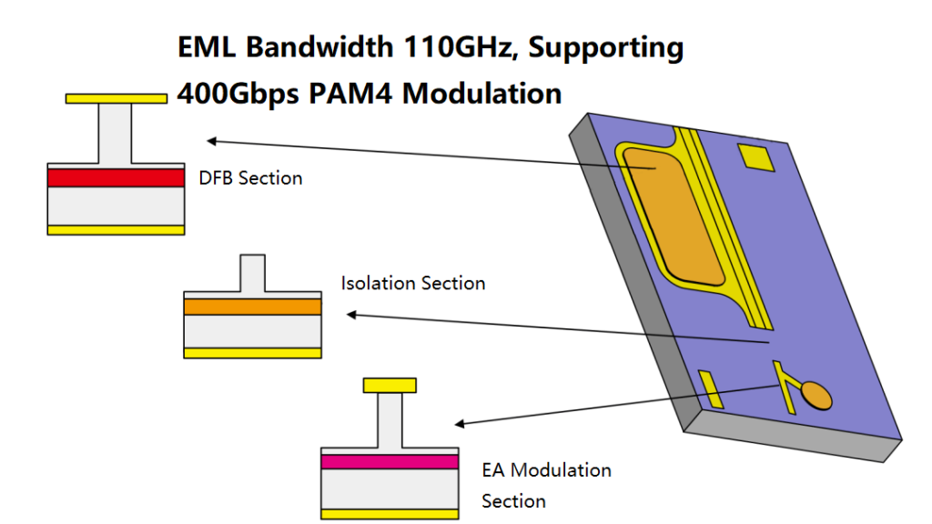
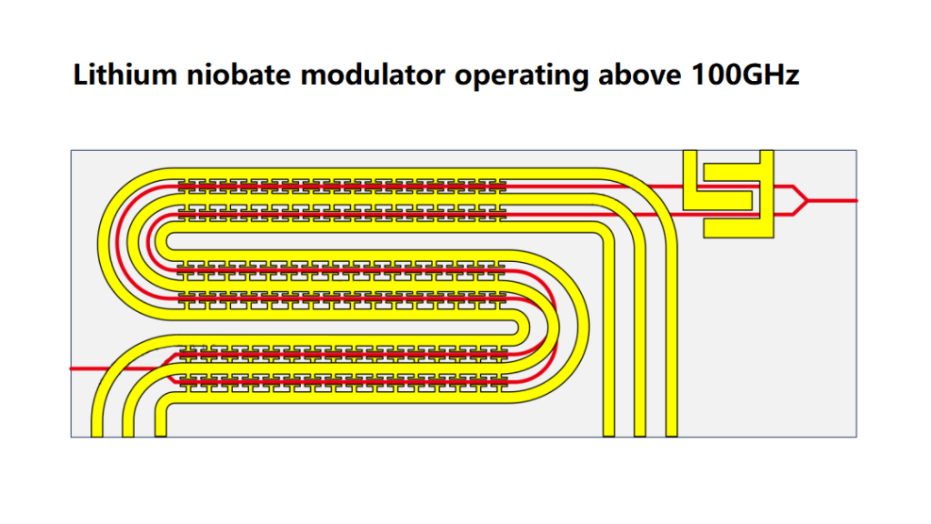
An accompanying diagram illustrates that HiSilicon’s EML bandwidth has reached 110 GHz this year, enabling support for modulation signal rates above 400 Gbps PAM4. With the adoption of higher-order modulation schemes, such as PAM6 and PAM8, bit rates exceeding 500 Gbps become feasible.
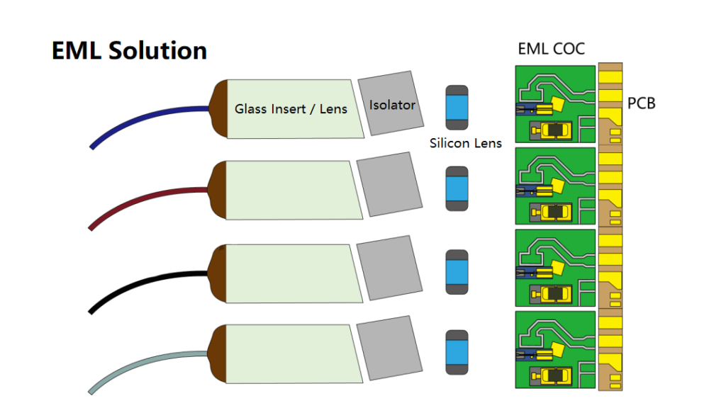
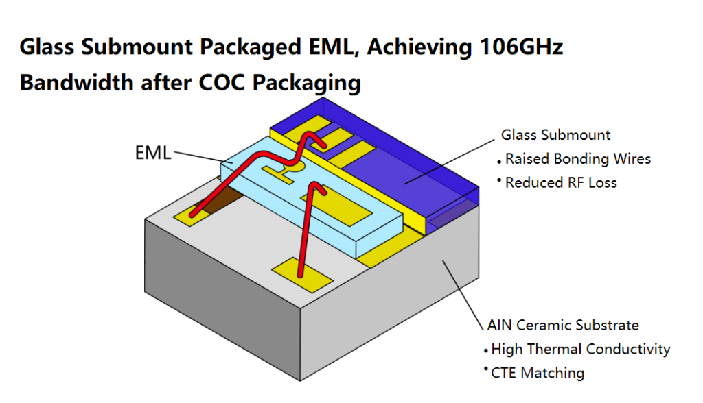
EML packaging is critically linked to its overall operational bandwidth, prompting extensive experimental investigations into various packaging methodologies.
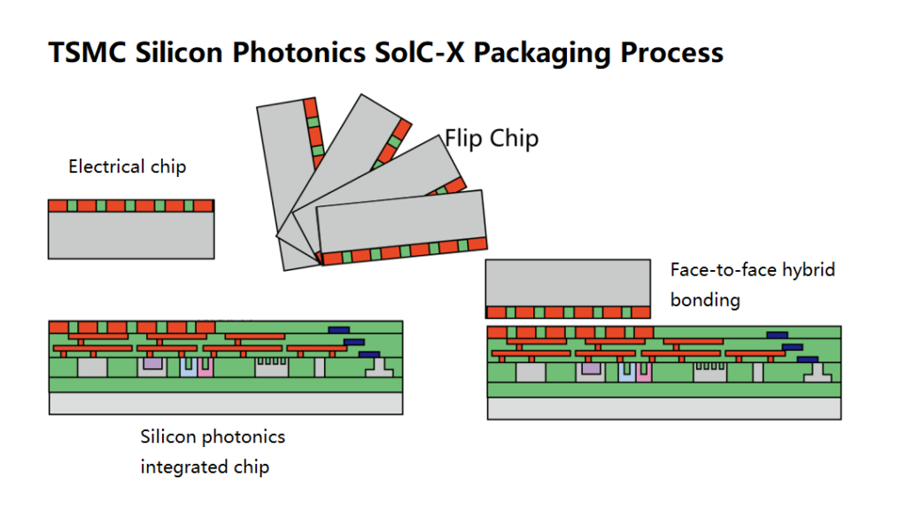
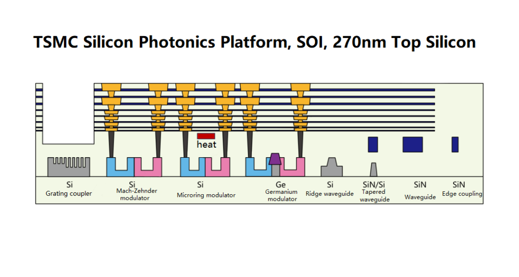
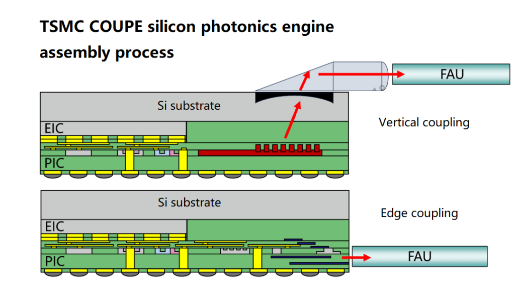
Silicon photonics has emerged as a preferred technological option not only due to its high level of integration but also because it offers substantial packaging bandwidth, exemplified by TSMC’s silicon photonics 3D packaging.
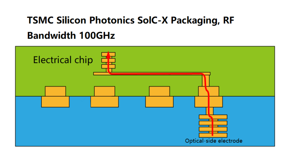
Although silicon photonic modules are applied in both hot-pluggable optical modules and CPO systems, and currently operate at the 224 Gbps PAM4 modulation rate, they are somewhat limited when compared to the bandwidth performance offered by EML.
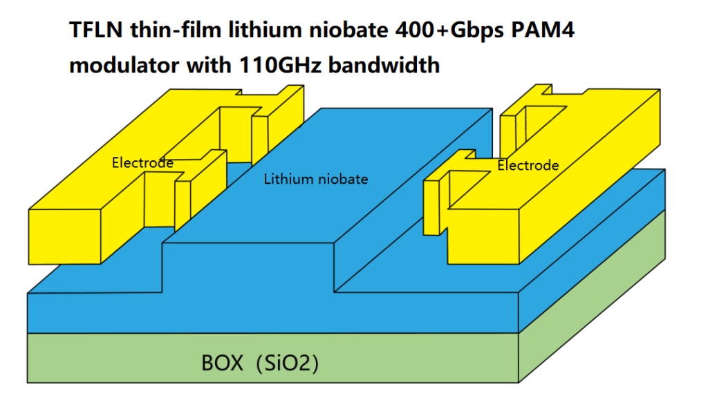
Moreover, while silicon photonics shows promise, its bandwidth is slightly inferior to that of EML. In response, researchers are exploring thin-film lithium niobate (TFLN), which offers a significantly greater optical bandwidth. The point of investigation is to determine whether, within an integrated platform, one can simultaneously leverage the substantial bandwidth afforded by silicon photonics’ packaging processes and realize a corresponding improvement in modulator bandwidth.
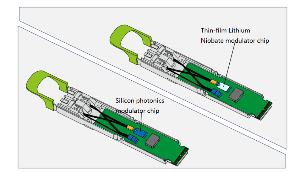
Some manufacturers are examining designs for lithium niobate modulators that can achieve bandwidths of 100 GHz or greater.
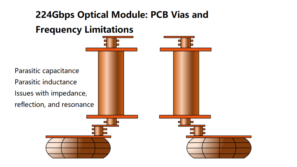
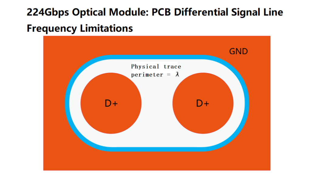
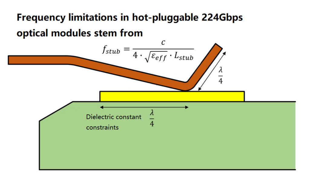
Processing 224 Gbps PAM4 signals presents considerable challenges. Both the optical chip and the PCB’s electrical signal processing must contend with numerous issues: parasitic parameters associated with vias, the layout and return path control of differential signals, the balancing of odd-mode and even-mode components, the effects of fiberglass, and differential signal skew. These factors contribute to noise, signal loss, and self-resonance in PCB circuitry. In addition, hot-pluggable optical modules face further constraints due to limitations in connector contact points relative to frequency.
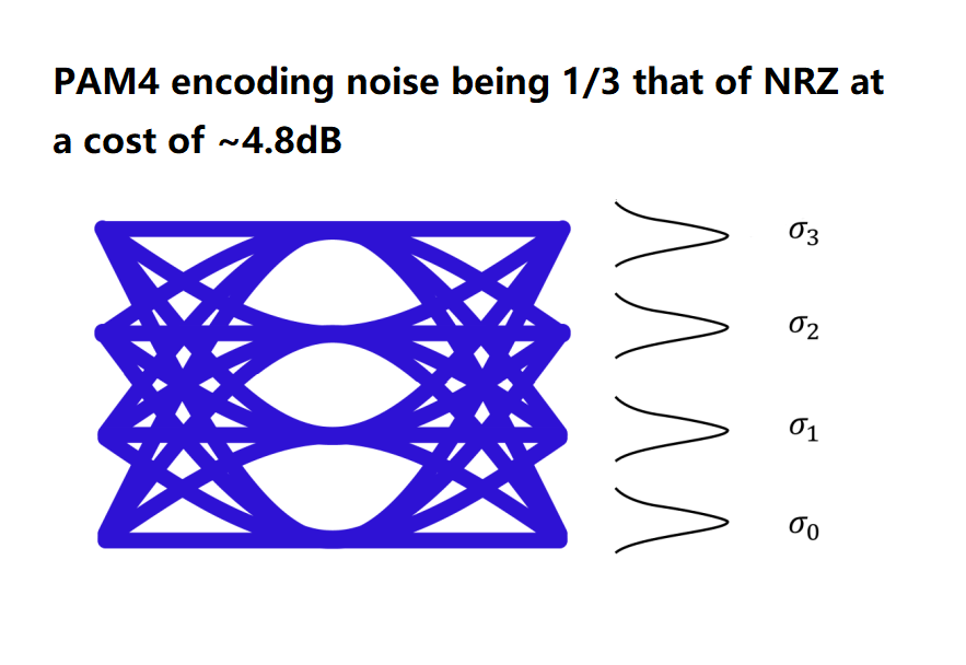
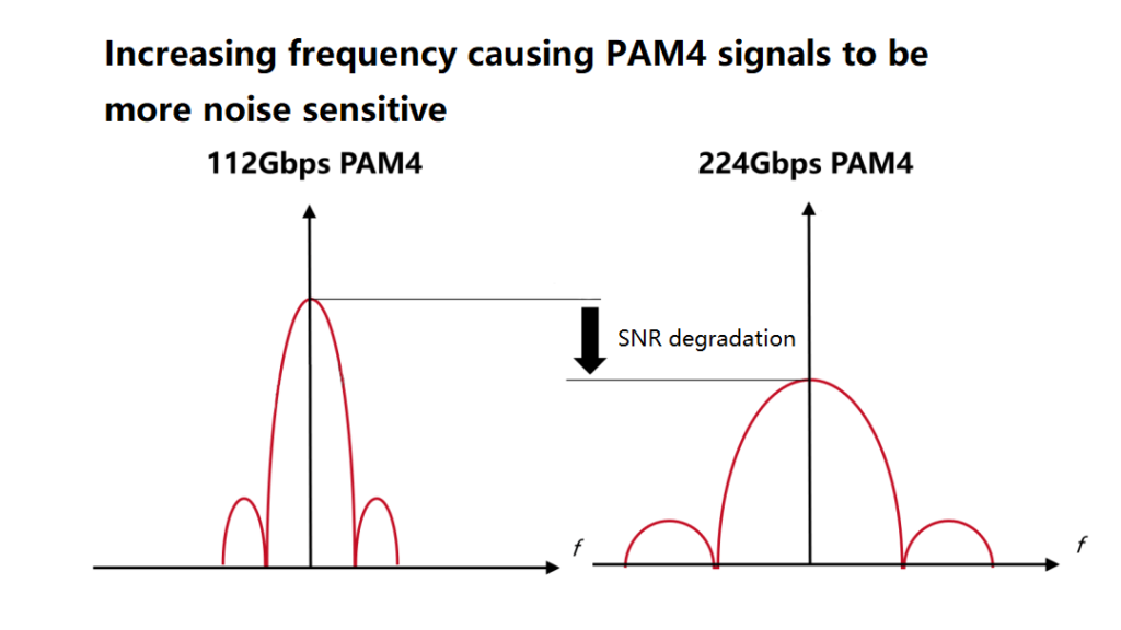
The challenges are compounded at higher speeds, such as in 800 G and 1.6 T optical modules, where signal processing becomes extremely demanding. PAM4 modulation is inherently sensitive to noise, and the encoding process contributes a degradation of approximately 4.8 dB to the signal-to-noise ratio (SNR).
As frequency increases, further degradation in SNR is observed.
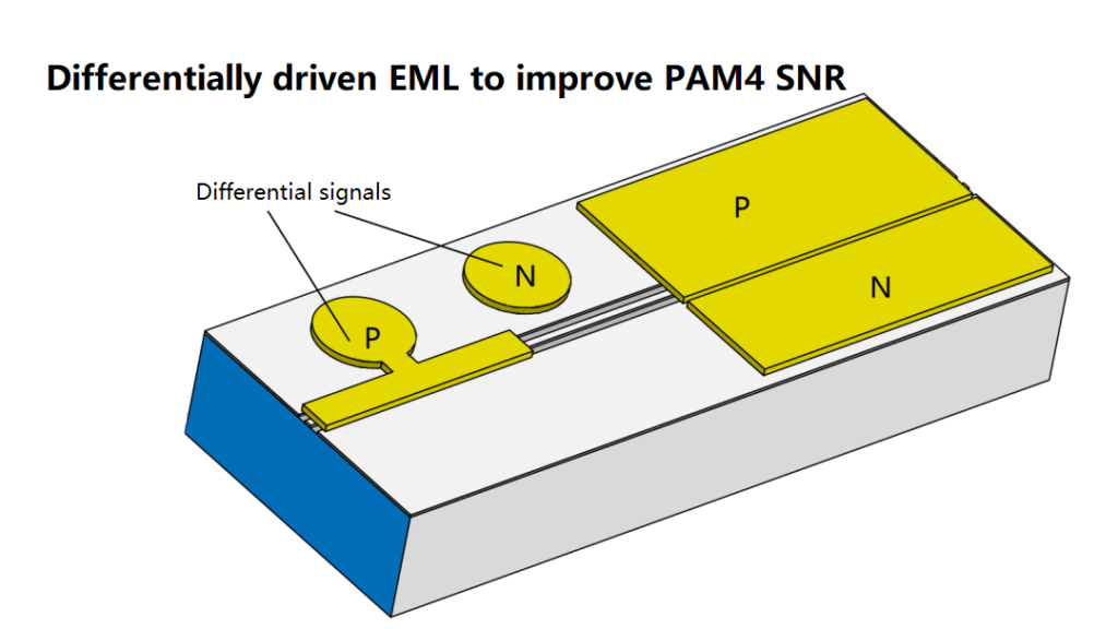
One approach to mitigate these issues is to increase the signal amplitude at the chip level—for example, by employing differential EML designs, which effectively improve the “numerator” (signal level) in the SNR equation.
Conversely, efforts must focus on reducing noise, thereby minimizing the SNR “denominator.”
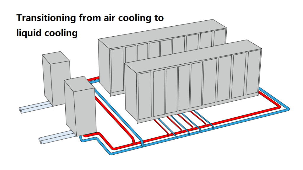
In addition to chip-level optimizations, digital signal processing (DSP) algorithms are used to optimize or compensate for SNR; however, these techniques generally result in significantly increased power consumption. Given that optical modules themselves have high power consumption, effective thermal management is essential, with liquid cooling solutions offering enhanced heat dissipation, which is particularly beneficial in AI applications.
Beyond traditional hot-pluggable optical modules, alternative approaches—such as Laser Package Optics (LPO) methods that eliminate the need for DSP, and low-power CPO designs—have gained prominence, with CPO emerging as an industry hotspot this year.
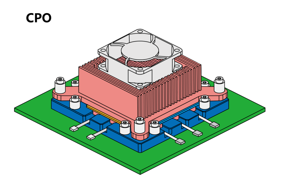
CPO solutions are available in both single-mode and multimode formats; multimode CPO typically employs VCSEL as the light source, whereas single-mode CPO is oriented toward silicon photonics. Silicon photonics integration technology presents substantial market opportunities in both hot-pluggable modules and CPO optical engines. Numerous manufacturers have launched their own silicon photonics platforms featuring a range of top-layer silicon choices in dimensions such as 160 nm, 220 nm, 270 nm, 300 nm, and 400 nm. Additionally, various forms of silicon nitride layers—whether single-layer or multi-layer—are employed. There are also diversified platforms that integrate technologies such as InP on silicon, GaAs on silicon, TFLN (lithium niobate) on silicon, and BTO (barium titanate) on silicon.
In addition to silicon photonics wafer-level processes, there exists a wide array of optical coupling designs and packaging technologies.
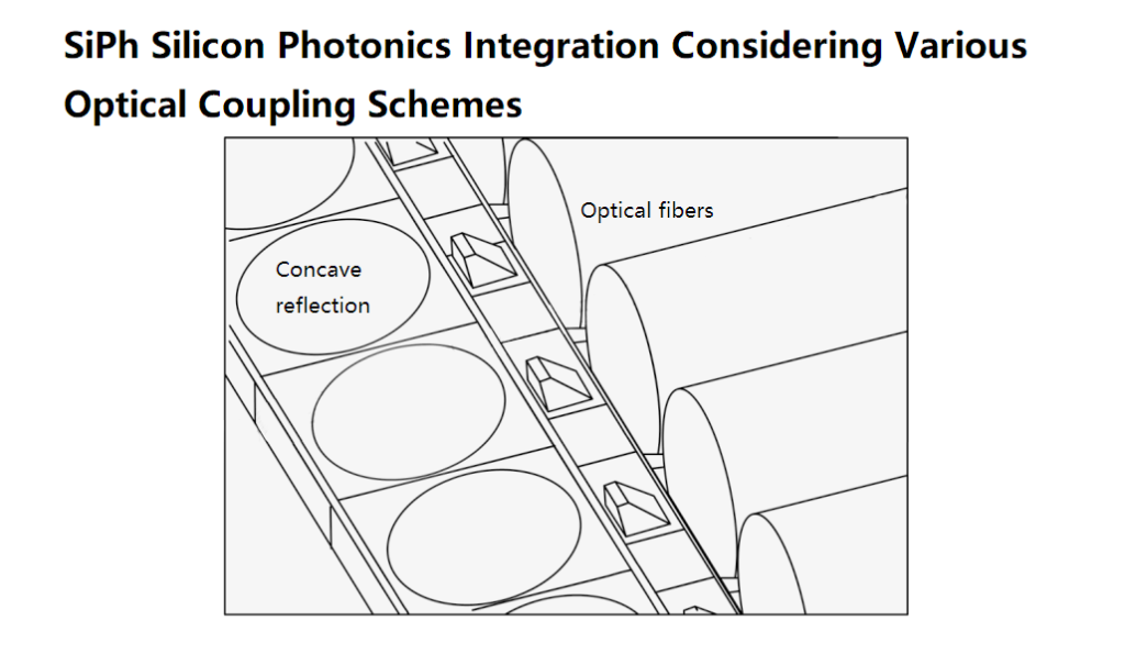
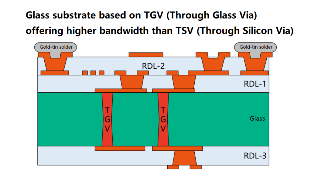
EML packaging may be implemented using silicon, ceramic, or glass substrates, while VCSELs may utilize packaging based on resin, ceramic, or glass substrates. Similarly, wafer-level packaging for integrated chips can be realized with resin-localized silicon substrates, full silicon substrates, or glass substrates. The aim is to achieve higher radio-frequency bandwidths through reduced via diameters and line widths—a goal that inherently introduces greater complexity and reliability challenges in the manufacturing process.
Related Products:
-
 NVIDIA MMA4Z00-NS Compatible 800Gb/s Twin-port OSFP 2x400G SR8 PAM4 850nm 100m DOM Dual MPO-12 MMF Optical Transceiver Module
$650.00
NVIDIA MMA4Z00-NS Compatible 800Gb/s Twin-port OSFP 2x400G SR8 PAM4 850nm 100m DOM Dual MPO-12 MMF Optical Transceiver Module
$650.00
-
NVIDIA MMA4Z00-NS-FLT Compatible 800Gb/s Twin-port OSFP 2x400G SR8 PAM4 850nm 100m DOM Dual MPO-12 MMF Optical Transceiver Module
$650.00
-
NVIDIA MMS4X00-NM Compatible 800Gb/s Twin-port OSFP 2x400G PAM4 1310nm 500m DOM Dual MTP/MPO-12 SMF Optical Transceiver Module
$900.00
-
NVIDIA MMS4X00-NM-FLT Compatible 800G Twin-port OSFP 2x400G Flat Top PAM4 1310nm 500m DOM Dual MTP/MPO-12 SMF Optical Transceiver Module
$1199.00
-
NVIDIA MMS4X50-NM Compatible OSFP 2x400G FR4 PAM4 1310nm 2km DOM Dual Duplex LC SMF Optical Transceiver Module
$1200.00
-
NVIDIA MMS4A00 (980-9IAH1-00XM00) Compatible 1.6T OSFP DR8D PAM4 1311nm 500m IHS/Finned Top Dual MPO-12 SMF Optical Transceiver Module
$2600.00