Huawei has recently made a significant impact on the industry with its innovative AI accelerator and rack-level architecture. China’s latest domestically developed cloud supercomputing solution, CloudMatrix M8, was officially unveiled. Built upon the Ascend 910C processor, this solution is positioned to directly rival Nvidia’s GB200 NVL72 system, exhibiting superior technological advantages in several key metrics compared to Nvidia’s rack-level offerings. The engineering breakthroughs are not confined merely to the chip level; they extend comprehensively across the accelerator architecture, network topology, optical interconnect technology, and software stack, among other system-level dimensions.
The Ascend 910C NPU features dual-die packaging, interconnected via a high-bandwidth bus. Each NPU’s single die integrates 7×224Gbps in the Unified Bus (UB) plane and provides 200Gbps unidirectional bandwidth in the RDMA plane. This architecture enables high-performance computing for AI workloads, ensuring efficient data processing and interconnectivity within the CloudMatrix 910C platform.
For SemiAnalysis, Huawei’s Ascend chips are far from unfamiliar. In an era where the overall system significance outweighs microarchitecture design alone, Huawei is continuously pushing the performance boundaries of artificial intelligence systems. Although certain technical trade-offs exist, within the context of export controls and limited domestic manufacturing capacity, China’s current export control framework still appears to have exploitable loopholes.
While Huawei’s chip technology may be one generation behind its competitors, its expansion solution is arguably a generation ahead of the current market offerings from Nvidia and AMD. The CloudMatrix 384 (CM384), for example, consists of 384 Ascend 910C chips interconnected through a fully connected topology. The design philosophy here is clear: by incorporating a quantity of Ascend chips that is five times greater, the solution effectively compensates for the fact that the performance of a single GPU is only one-third that of Nvidia’s Blackwell series.
The CloudMatrix 384 super node employs a sophisticated network topology with three complementary planes: the UB plane for non-blocking all-to-all interconnects among 384 NPUs and 192 CPUs, the RDMA plane for scale-out communication using RoCE with up to 400Gbps per NPU, and the VPC plane for broader data center connectivity. This design supports ultra-large-scale computing clusters, enabling efficient collaboration for AI-driven applications.
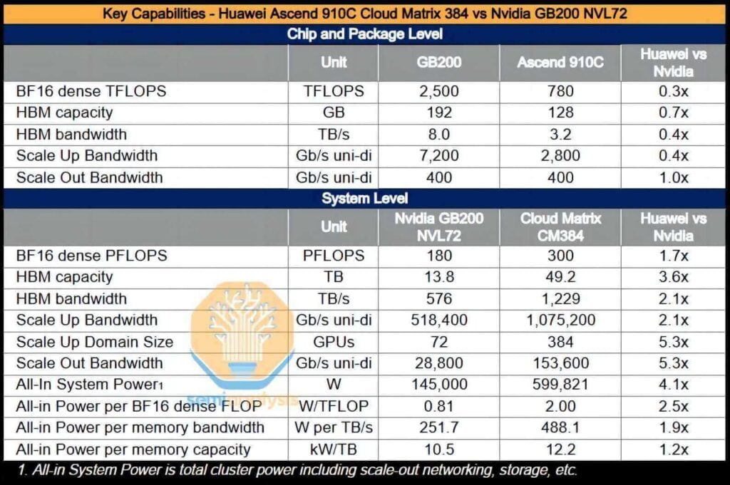
The complete CloudMatrix system is capable of delivering an intensive BF16 computing performance of 300 petaflops, nearly twice that of the GB200 NVL72. With over a 3.6-fold increase in total memory capacity and a 2.1-fold increase in memory bandwidth, Huawei—and by extension China—now possesses the capability to deploy AI systems that surpass those provided by Nvidia.
Furthermore, the CM384 is particularly well aligned with areas where China holds distinct advantages, such as domestic network production capabilities, infrastructure software designed to mitigate network failures, and the potential for scaling up to larger applications through improvements in manufacturing yield. However, the solution is not without its drawbacks: it exhibits power consumption that is 3.9 times higher than that of the GB200 NVL72, with per-FLOP efficiency reduced by a factor of 2.3, memory bandwidth efficiency (per TB/s) lower by 1.8 times, and per-TB high-bandwidth memory (HBM) capacity efficiency decreased by 1.1 times.
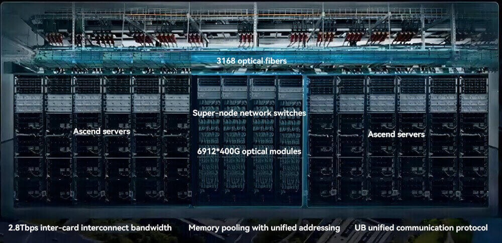
The CloudMatrix 384 super node utilizes 6,912 400G optical modules to build a high-bandwidth, low-latency optical interconnect network. The UB plane requires 5,376 modules to connect 384 NPUs, with each NPU using 7 modules bidirectionally. The RDMA plane uses 1,536 modules, including 384 for server NICs, 768 for leaf-layer switches, and 384 for spine-layer switches in a two-layer fat-tree architecture. This precise allocation ensures non-blocking communication and scalability for large-scale AI and scientific computing workloads.
Despite these shortcomings in energy efficiency, the power consumption issue is not a critical constraint within the Chinese context. Whereas the West often argues that artificial intelligence development is limited by electricity supply, China’s situation is quite the opposite. Over the past decade, while Western countries have dedicated significant efforts to transition their coal-dependent power infrastructures to more environmentally friendly natural gas and renewable energy sources—and to improve per capita energy efficiency—China faces mounting demands for electrical power due to an elevated standard of living and extensive large-scale investments.
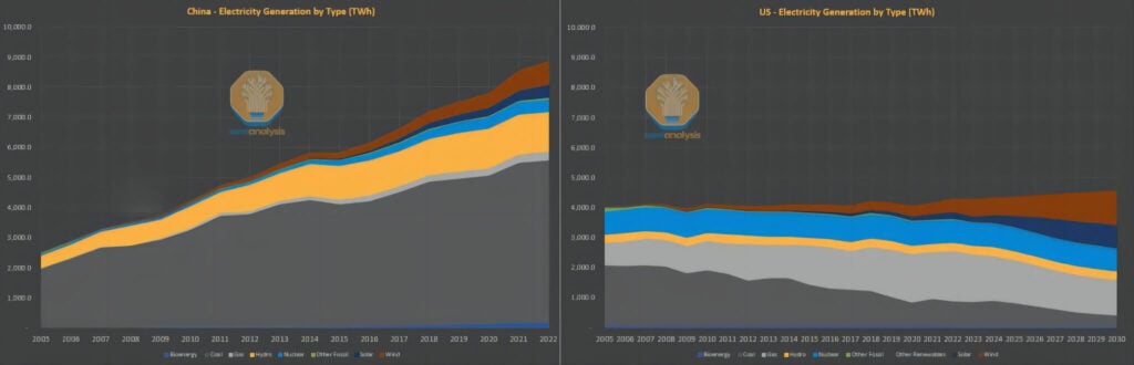
Although China’s energy system has traditionally relied heavily on coal, the nation now leads the world in installed capacities of solar, hydropower, and wind power, and it is currently at the forefront of nuclear power deployment. In contrast, the United States’ nuclear capacity remains at levels reminiscent of the 1970s. In short, the upgrade and expansion capabilities of the American power grid have markedly diminished, whereas the additional grid capacity introduced in China since 2011 is comparable to the entire scale of the U.S. grid.
In a scenario where electricity is relatively abundant and energy consumption constraints are less critical, it becomes a logical engineering decision to forgo stringent power density requirements in favor of broader scaling, especially when incorporating advances such as optical interconnect technology in the design. Indeed, the CM384’s design even accounts for system-level constraints extending beyond the rack. It is our view that the limitations on China’s AI ambitions are not determined solely by power supply concerns; Huawei’s solution continues to offer various avenues for sustained and scalable expansion.
A common misconception is that the Huawei 910C chip is manufactured entirely within China. Although the design process is fully domestically executed, actual production remains heavily reliant on foreign inputs. Whether it is Samsung’s high-bandwidth memory (HBM) or equipment from the United States, the Netherlands, or Japan, the production process still depends significantly on the global supply chain.
Huawei’s HBM Procurement Path
China’s dependence on external sources in cutting-edge technological areas is only part of the challenge; its reliance on high-bandwidth memory (HBM) is even more acute. Currently, China has not yet achieved stable, domestic mass production of HBM—Changxin Storage (CXMT) is expected to require a minimum of one more year to reach scale. Fortunately, Samsung has emerged as the core supplier of HBM for China, and as a result, Huawei has preemptively stockpiled 13 million HBM stacks, a quantity sufficient for packaging 1.6 million Ascend 910C chips. Notably, this accumulation occurred prior to the enforcement of the HBM export ban.
It is also noteworthy that banned HBM components continue to flow back into China through gray channels. The current HBM export restrictions apply only to original HBM packaging units; chips incorporating HBM can still be legally transported, provided that they do not exceed the stipulated floating-point operations (FLOPS) limits. In this regard, Samsung’s sole distributor in the Greater China region, CoAsia Electronics, has persistently supplied HBM2E to the ASIC design service company Faraday. Faraday then utilizes SPIL (Siliconware Precision) to package these memory components with cost-effective 16nm logic chips.
Subsequently, Faraday ships the finished product to China in a system-level package. Although this practice adheres to technical regulations, the design incorporates extremely low-intensity, low-temperature solder bumps, which allow the HBM to detach from the package easily. In essence, the so-called “packaging” in this case amounts to a loosely integrated and almost formalized assembly.
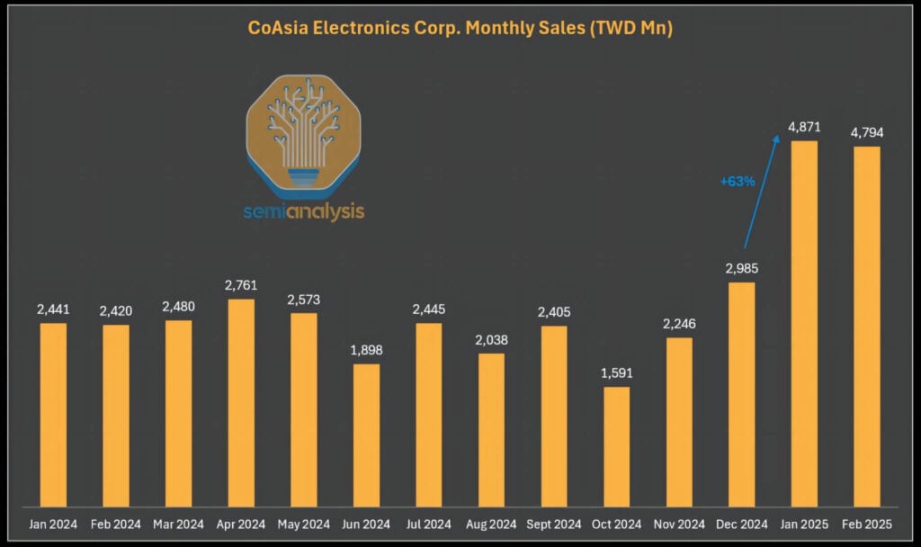
Since the export controls took effect in 2025, CoAsia Electronics’ revenues have surged sharply—a development that appears to be anything but coincidental.
China’s Domestic Foundries Retain Growth Potential
Although the Chinese semiconductor industry still relies on overseas production, its domestic supply chain capabilities have improved rapidly and have long been underestimated. We continue to monitor the manufacturing strengths of SMIC (Semiconductor Manufacturing International Corporation) and CXMT (ChangXin Memory Technologies) closely. Despite ongoing challenges related to yield and capacity, the long-term trajectory toward the scalable production of Chinese GPUs remains noteworthy.
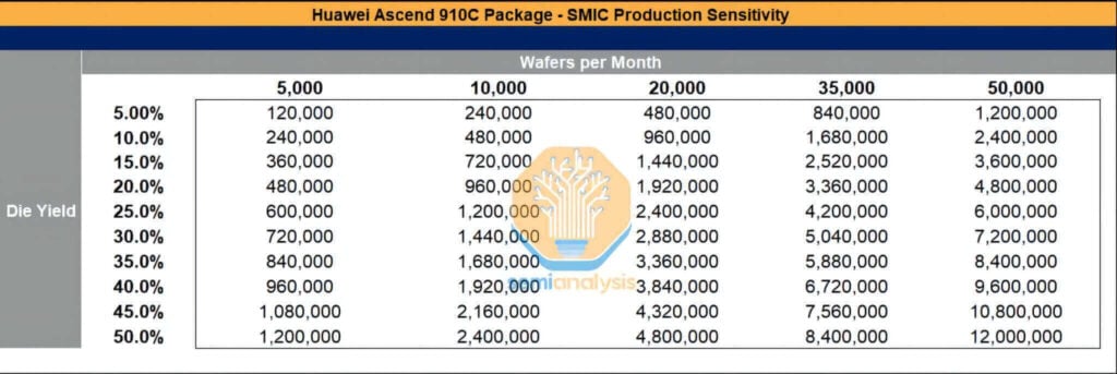
Even under the pressure of sanctions, both SMIC and CXMT have secured manufacturing equipment worth tens of billions of dollars, while they continue to import substantial quantities of exclusively sourced chemicals and materials from abroad. SMIC, for instance, is expanding its advanced process capacity in Shanghai, Shenzhen, and Beijing. Its monthly wafer production is projected to approach 50,000 units this year, and sustained expansion is further driven by the continuous acquisition of overseas equipment, coupled with the less-than-rigorous enforcement of sanctions. Should yield rates improve, the packaging volume of the Ascend 910C chips could reach considerable levels.
Although TSMC has already allocated 2.9 million wafers for production in 2024–2025—representing enough capacity to produce approximately 800,000 Ascend 910B chips and 1.05 million Ascend 910C chips—the potential for SMIC to experience explosive capacity growth remains if high-bandwidth memory (HBM), wafer fabrication equipment, equipment maintenance resources, and essential chemicals (such as photoresist) are not effectively regulated.
CloudMatrix 384 System Architecture
The following analysis delves into the architectural design of the CloudMatrix 384 system, examining its vertical and horizontal expansion networks, power consumption budgeting, and overall cost structure.
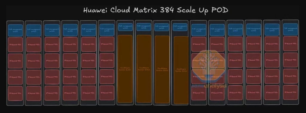
The complete CloudMatrix system is distributed across 16 racks. Of these, 12 computing racks each mount 32 GPUs, while four additional racks situated centrally serve as vertical expansion switch racks. To achieve a hyperscale cluster, Huawei employs a cross-rack vertical expansion approach that integrates optical communication technology—a strategy that enables full interconnection among hundreds of GPUs, though it presents considerable technical challenges.
Similarity with the DGX H100 NVL256 “Ranger”
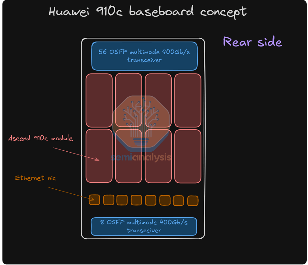
As early as 2022, Nvidia introduced the DGX H100 NVL256 “Ranger” platform; however, the system never reached mass production. This was due to prohibitive cost, excessive power consumption, and inherent reliability issues arising from an overabundance of optical transceiver requirements and a dual-layer network architecture. In contrast, the Huawei CloudMatrix Pod takes a more extreme approach: its network design requires 6,912 units of 400G Linear Pluggable Optical (LPO) modules, the vast majority of which facilitate vertical expansion network interconnectivity.
Evaluation of the CloudMatrix 384 Vertical Expansion Topology
This section provides an in-depth evaluation of Huawei’s vertical expansion rack architecture across 384 chips—a design positioned to rival NVLink. The analysis covers both vertical and horizontal expansion networks, a comprehensive breakdown of system power consumption, and an assessment of how the large-scale application of optical modules (and the corresponding absence of copper cables) impacts overall performance and cost. Notably, the discussion also addresses the cost implications associated with Huawei’s extensive deployment of LPO modules.
Core Parameters
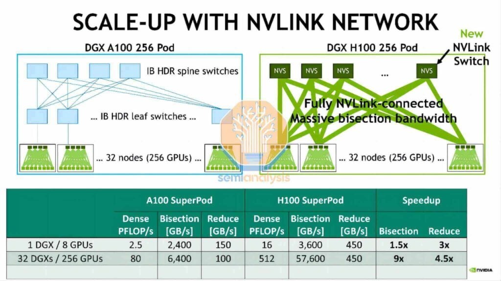
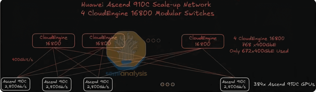
Each Huawei Ascend 910C GPU offers a unidirectional vertical expansion bandwidth of 2,800 Gbit/s, a figure that is of a similar order of magnitude to the 7,200 Gb/s vertical expansion bandwidth provided by Nvidia’s GB200 NVL72 per GPU. Whereas the Nvidia NVL72 achieves its vertical network interconnection via high-density, direct copper cabling, Huawei adopts a more straightforward approach—deploying seven 400G optical transceivers per GPU in a stacked configuration to reach the 2,800 Gbit/s figure.
This strategy, however, comes at a higher cost, with significantly increased power consumption, and presents challenges related to airflow management and the ease of installation and maintenance. Despite these hurdles, the approach successfully meets the system’s functional objectives. The vertical expansion network itself employs a single-layer architecture to interconnect all GPUs through 16,800 modular switches arranged in a flat, single-tier topology. These switches utilize Huawei’s proprietary line cards and switching matrix planes, employing a cell spraying mechanism similar to that of Broadcom’s Jericho3 line cards paired with the Ramon3 switching matrix cards found in Arista modular switches.
Vertical Optical Interconnect Expansion and Copper-Free Design
Deploying 5,000 optical modules for vertical expansion may lead to reliability issues. To mitigate this, high-quality fault-tolerant training software is required to address the potential failures that can arise from such a large-scale deployment of optical modules.
Each CloudMatrix 384 Pod is equipped with a total of 6,912 400G optical modules/transceivers. Of these, 5,376 are allocated for the vertical expansion network, while the remaining 1,536 serve the horizontal expansion network.
A single Pod contains 384 Ascend 910C chips, each providing an interconnect bandwidth of 2.8 Tbps for vertical expansion communications. Consequently, each chip requires seven 400G transceivers, resulting in 384 GPUs × 7 = 2,688 transceivers per Pod. Given the single-layer flat topology, the switch side must mirror this deployment with 2,688 transceivers, leading to a total use of 5,376 400G transceivers in the vertical expansion network.
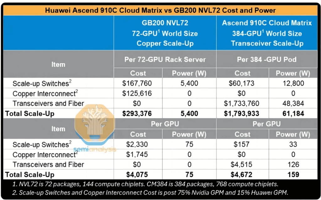
If 400G Linear Pluggable Optical (LPO) transceivers—priced below $200 each and consuming approximately 6.5W per module—are used, the total cost of ownership (TCO) of the supernode’s vertical expansion network would be approximately six times that of an NVL72 rack, with power consumption exceeding ten times that of the NVL72. Even on a per-GPU basis, although the power consumption is twice that of the NVL72 and the cost remains relatively comparable, the computational performance reaches only 30% of that offered by NVL72.
CloudMatrix 384 Horizontal Expansion Topology Evaluation
The CloudMatrix 384 adopts a dual-layer, 8-track optimized topology. Each CloudEngine modular switch for horizontal expansion is equipped with 768 400G ports—384 of which connect downward to 384 GPUs, while the other 384 ports are reserved for upward interconnection. Since each Pod contains 384 GPUs (each equipped with a 400G network interface card), an additional leaf switch is required for access beyond the provision of 0.5 spine switches.
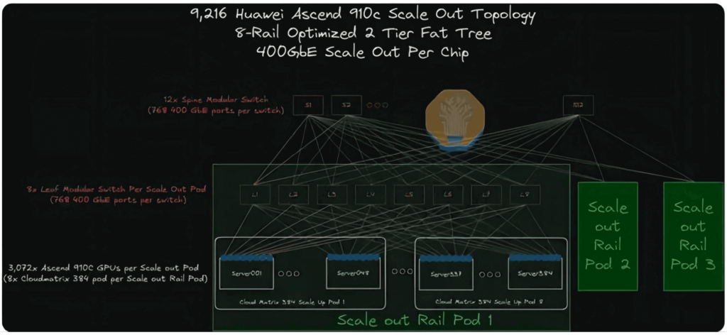
The calculation of transceivers for this network is straightforward:
- GPU Side: 384 400G transceivers are needed (one per GPU);
- Leaf Layer: Since half of the ports are used for upward connection (linking GPUs with the spine layer), the number of transceivers required must be doubled;
- Total: The horizontal expansion network therefore requires 384 × 4 = 1,536 400G transceivers.
LPO Transceivers
One potential measure proposed by Huawei to reduce overall cluster power consumption is the adoption of Linear Pluggable Optical (LPO) modules for optical transmission. LPO modules are designed to transmit data directly via optical signals without the need for an internal digital signal processor (DSP). In contrast to conventional transceivers, which convert analog signals to digital for timing calibration/recovery before converting them back to analog, LPO modules perform a direct linear transmission of electrical signals from the host to the optical device. This design simplifies the internal architecture of the module, yielding over a 30% reduction in both power consumption and cost. However, because a large number of transceivers are still required, the overall power consumption of the CM384 cluster remains significantly higher compared to that of the NVL72.
Chip Level
Huawei’s Ascend 910B and 910C accelerators represent the pinnacle of domestically produced Chinese GPUs. Despite facing certain technological constraints, their performance remains outstanding. At the chip level, however, their performance does not yet match that of comparable NVIDIA products.
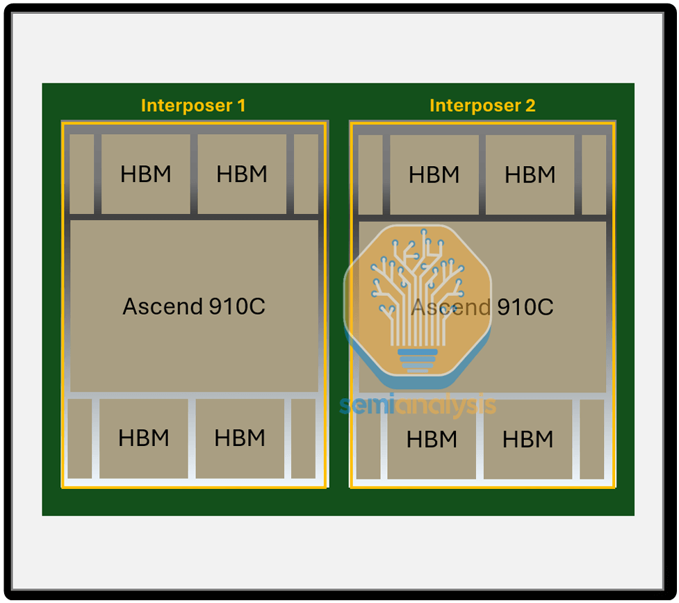
The Ascend 910C is an iteration of the 910B, integrating the interposer layers of two 910B chips onto a single substrate. This integration effectively doubles the single-chip computing performance as well as the memory bandwidth.
System-Level Power Consumption Estimate
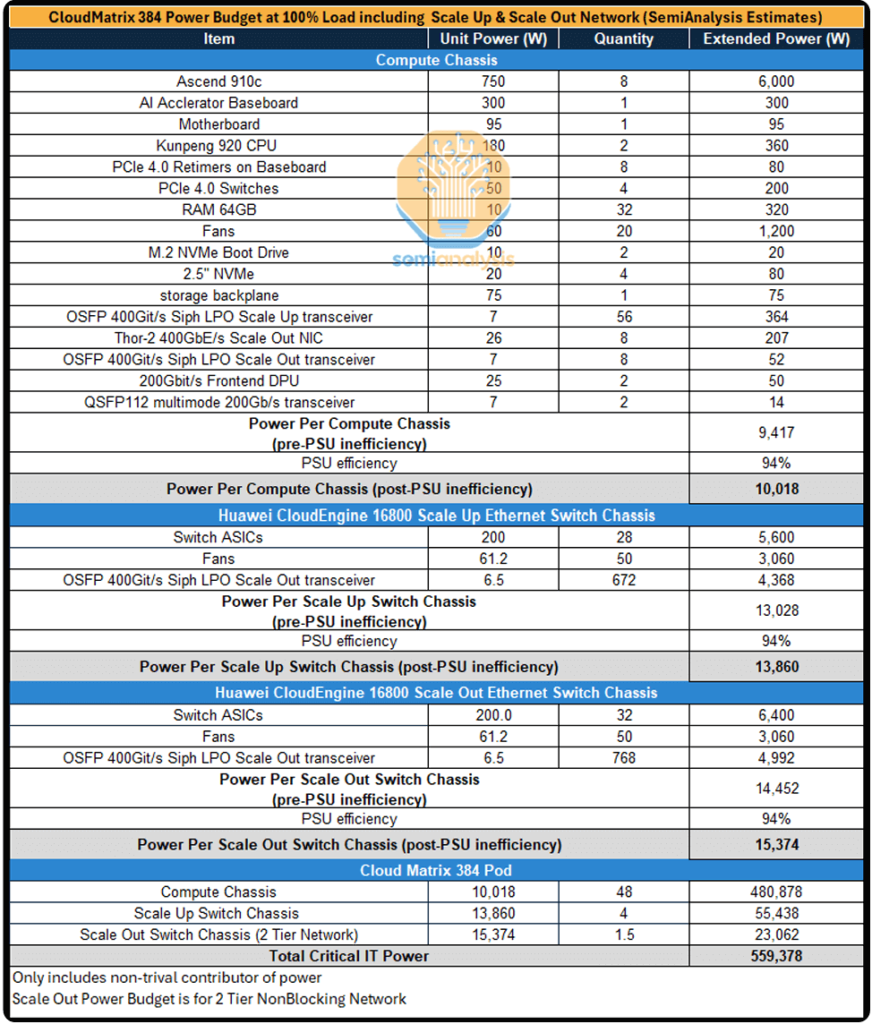
Due to the extensive deployment of optical transceivers in both the vertical and horizontal expansion networks, the power consumption of a cluster containing 384 GPUs is exceedingly high. It is estimated that a single CM384 supernode consumes nearly 500 kilowatts, more than four times the approximate 145 kilowatts consumed by an NVIDIA GB200 NVL72 rack.
Single-GPU Energy Efficiency Comparison
On an individual GPU basis, the overall power consumption of Huawei GPUs is approximately 70%–80% of that of NVIDIA NVL72 B200 GPUs. In terms of overall supernode performance, the Huawei solution delivers 70% higher floating-point operations per second (FLOPS) compared to the NVL72. However, the architectural design introduces the following energy efficiency disadvantages:
- Power Consumption per FLOP: 2.3 times higher,
- Power Consumption per TB/s of Memory Bandwidth: 1.8 times higher,
- Power Consumption per TB of HBM Memory Capacity: 1.1 times higher.

These additional expenditures and higher power consumption represent costs that China must incur in its efforts to match Western computational performance levels. Given China’s abundant energy reserves and the significance of national security in such projects, these costs are considered relatively manageable. China’s energy advantage will likely serve as a critical asset, enabling data centers to expand in both scale and speed.
Related Products:
-
 OSFP-400G-SR8 400G SR8 OSFP PAM4 850nm MTP/MPO-16 100m OM3 MMF FEC Optical Transceiver Module
$400.00
OSFP-400G-SR8 400G SR8 OSFP PAM4 850nm MTP/MPO-16 100m OM3 MMF FEC Optical Transceiver Module
$400.00
-
OSFP-400G-DR4 400G OSFP DR4 PAM4 1310nm MTP/MPO-12 500m SMF FEC Optical Transceiver Module
$800.00
-
OSFP-400G-PSM8 400G PSM8 OSFP PAM4 1550nm MTP/MPO-16 300m SMF FEC Optical Transceiver Module
$1000.00
-
OSFP-400G-SR4-FLT 400G OSFP SR4 Flat Top PAM4 850nm 30m on OM3/50m on OM4 MTP/MPO-12 Multimode FEC Optical Transceiver Module
$550.00
-
OSFP-400G-DR4-FLT 400G OSFP DR4 Flat Top PAM4 1310nm MTP/MPO-12 500m SMF FEC Optical Transceiver Module
$700.00
-
QSFP112-400G-SR4 400G QSFP112 SR4 PAM4 850nm 100m MTP/MPO-12 OM3 FEC Optical Transceiver Module
$450.00
-
QSFP112-400G-DR4 400G QSFP112 DR4 PAM4 1310nm 500m MTP/MPO-12 with KP4 FEC Optical Transceiver Module
$850.00
-
QSFP112-400G-FR1 4x100G QSFP112 FR1 PAM4 1310nm 2km MTP/MPO-12 SMF FEC Optical Transceiver Module
$1200.00
-
NVIDIA MMA4Z00-NS400 Compatible 400G OSFP SR4 Flat Top PAM4 850nm 30m on OM3/50m on OM4 MTP/MPO-12 Multimode FEC Optical Transceiver Module
$550.00
-
NVIDIA MMS4X00-NS400 Compatible 400G OSFP DR4 Flat Top PAM4 1310nm MTP/MPO-12 500m SMF FEC Optical Transceiver Module
$700.00
-
NVIDIA MMA1Z00-NS400 Compatible 400G QSFP112 VR4 PAM4 850nm 50m MTP/MPO-12 OM4 FEC Optical Transceiver Module
$550.00
-
NVIDIA MMS1Z00-NS400 Compatible 400G NDR QSFP112 DR4 PAM4 1310nm 500m MPO-12 with FEC Optical Transceiver Module
$850.00