In the fast-paced world of data communication, the demand for efficient, high-bandwidth solutions has never been greater. As AI-driven applications and massive data processing push the boundaries of network performance, optical modules and their integral optical module PCBs have evolved rapidly to meet these challenges. This evolution not only enhances transmission efficiency but also ensures reliability in demanding environments like data centers and cloud computing setups.
At FiberMall, we specialize in delivering cost-effective optical communication products and solutions, empowering global data centers, cloud environments, enterprise networks, access networks, and wireless systems. Our leadership in AI-enabled communication networks makes us the perfect partner for high-quality, value-driven optical modules and PCBs. In this blog, we’ll explore the background, technological advancements, and composition of optical modules, followed by a deep dive into optical module PCB essentials.
Background: The Surge in Demand for High-Bandwidth Networks
As is well known, demand drives development. The rapid advancement of optical modules stems directly from humanity’s growing need for efficient transmission of increasingly complex and voluminous data. This has, in turn, led to continually evolving and more complex technical requirements for optical module PCBs.
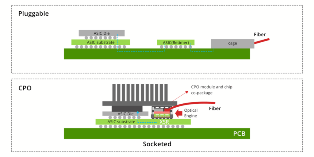
The rise of AI large-scale model training and inference has amplified the demand for massive parallel data computing, placing unprecedented pressure on global network bandwidth. This has accelerated the iteration of optical modules, while propelling emerging technologies like CPO, LPO, and Silicon Photonics to the forefront.
- CPO (Co-packaged Optics): This co-packaged optics technology focuses on integrating photonic and electronic components in a single package, ideal for high-speed, high-density interconnect transmission scenarios.
- LPO (Linear Pluggable Optics): Emphasizing pluggability and cost-effectiveness, LPO is suited for short-distance transmission applications.
- Silicon Photonics Technology: A method of fabricating optoelectronic devices using silicon materials, it combines the advantages of photonics and electronics for superior performance.
These innovations are reshaping optical communication solutions, ensuring seamless scalability for modern infrastructures.
Evolution Path of Optical Module Technologies
In the era of computing power, optical modules must deliver low power consumption and high bandwidth to support AI and big data workloads. Current industry trends point to the following evolution paths, transitioning from traditional pluggable modules to more integrated solutions that reduce power usage by up to 40% and latency by around 50%. This shift marks a pivotal move from pluggable-dominated designs to integrated-evolving optical interconnects, with LPO serving as an evolutionary step for pluggable modules and CPO representing the final, revolutionary form leveraging silicon photonics for minimized costs and power.
The table below outlines key emerging technologies in the evolution of optical modules, based on insights from ZTE’s “Data Center Optical Module Technology and Evolution.” It highlights technology names, detailed content, and summaries for each, providing a comprehensive view of how these advancements address high-density, low-power needs in AI-driven data centers:
| Technology Name | Content | Summary |
| Liquid-Cooled Optical Modules | In cold plate liquid cooling systems, the coolant does not directly contact heat-generating electronic components, so conventional optical modules generally do not need to consider compatibility issues when applied in such systems. However, the coolants in immersion and spray liquid cooling systems directly contact heat dissipation devices—especially in immersion systems, where devices are fully submerged in coolant. Conventional optical modules are designed for air-cooling scenarios and may fail in immersion or spray environments. Thus, targeted designs for liquid cooling and standardized technical requirements are essential to ensure reliable data transmission in these setups. | Liquid cooling offers ultra-high energy efficiency and heat density, serving as a key solution to data center heat dissipation pressures and energy-saving challenges. Liquid-cooled optical modules represent the inevitable trend. |
| LPO Solution | LPO replaces traditional DSP with linear direct drive technology, integrating functions into the switch chip and retaining only the driver chip (Driver) and transimpedance amplifier (TIA) chip. The Driver and TIA chips in LPO optical modules feature enhanced performance for improved linearity. | LPO excels in short-distance, low-power, low-latency applications, ideal for AI computing centers. Leveraging existing mature optical module supply chains, LPO can achieve rapid deployment with strong support from high-linearity TIA/Driver vendors. |
| CPO Solution | CPO co-packages optical engines and switch chips without using pluggable optical module formats. This enables faster electrical signal transmission between the engine and chip, shortening distances to reduce size, lower power consumption, and boost efficiency. | CPO reduces costs and power via switch optoelectronic co-packaging, offering the optimal comprehensive solution for future high-integration, low-power, low-cost, and ultra-high-rate module applications. |
| Silicon Photonics Technology | This low-cost, high-speed optical communication technology is based on silicon photonics, utilizing silicon-based complementary metal oxide semiconductor (CMOS) microelectronics processes for integrated photonic device fabrication. It merges CMOS’s ultra-large-scale logic and high-precision manufacturing with photonics’ ultra-high rates and low power (under CPO/LPO architectures). | Though R&D investments and sales lag behind III-V materials, with challenges in performance, process, and cost, silicon photonics’ cost and power advantages position it as the future mainstream optical device technology. |
| Thin-Film Lithium Niobate Technology | Compared to traditional bulk lithium niobate, thin-film lithium niobate waveguides enable sub-micron-scale optical waveguides, enhancing integration, light field confinement, and material interactions for ultra-high electro-optic bandwidth, ultra-low drive voltage, and ultra-low optical loss. This could revolutionize electro-optic modulators. | As a core device for ultra-high-speed data centers and coherent optical transmission, it offers high performance, low cost, small size, mass producibility, and CMOS compatibility—making it a highly competitive solution for future high-speed optical interconnects. |
| Coherent Sinking (Coherent Lite) | Within data centers, intensity modulation direct detection (IM-DD) remains dominant. To address IM-DD’s limitations in evolving demands, the industry is developing “coherent lite” solutions tailored for shorter-distance data center links. | As intra-data center connections exceed 1.6T toward 3.2T, dispersion and link budgets challenge IM-DD. Coherent lite emerges as a strong contender for large-scale 3.2T interconnects. |
| Light In Light Out (OIO) Technology | OIO is a chip-based optical interconnect integrated with computing chips (CPUs, GPUs, TPUs) in the same package for seamless communication in distributed systems (across boards, racks, and rows). It matches on-package electrical interconnects in bandwidth density, energy cost, and latency. Forms include on-board optics (OBO), NPO, CPO, and future optoelectronic integrated circuits (OEIC). OIO promises 100x+ channel density and bandwidth per channel, essential for switch chip evolution to 100T, 200T, or higher. | OIO is poised to enable unprecedented scalability in high-capacity networks, driving the next era of efficient, low-latency optical interconnects. |
This path underscores the shift toward more efficient, compact designs that minimize latency and energy use, critical for optical module PCBs in high-performance setups.
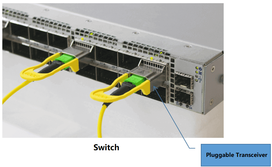
Composition of Optical Modules
Optical modules are assembled from optical chips and devices, then inserted or embedded into optical communication equipment for external connectivity. In fiber optic communication, they facilitate the mutual conversion between electrical and optical signals: electro-optical conversion at the transmitter end and opto-electrical conversion at the receiver end.
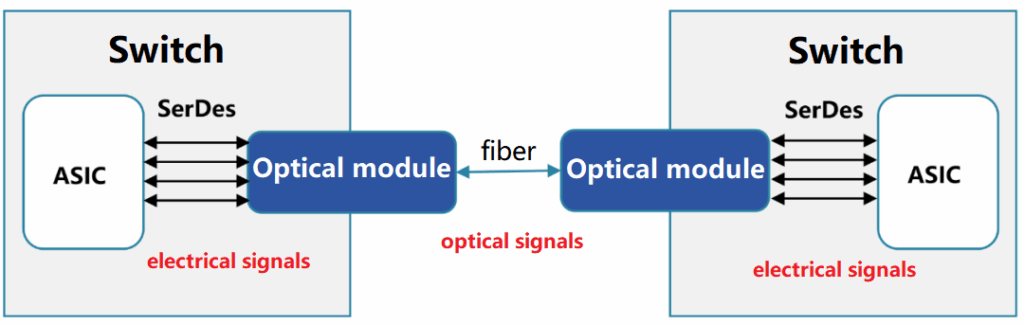
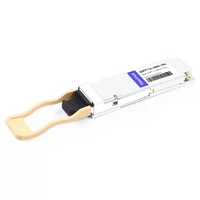
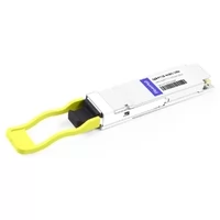
The core structure of an optical module comprises four key components:
- PCBA (Printed Circuit Board Assembly): The foundational board that integrates electrical components.
- TOSA (Transmitter Optical Sub-Assembly): Handles the transmission of optical signals.
- ROSA (Receiver Optical Sub-Assembly): Manages the reception and conversion of optical signals.
- Housing: Provides protection and structural integrity.
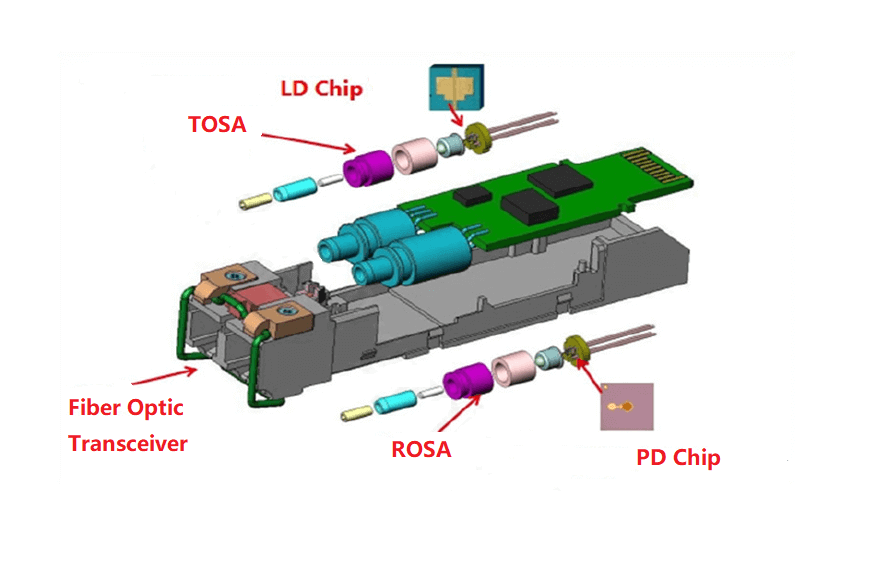
These elements work in harmony to ensure robust signal integrity, making optical module PCBs the unsung heroes of reliable data flow.
Optical Module PCBs: Meeting the Demands of the Computing Era
With the computing era’s emphasis on low power consumption and high bandwidth, the technical requirements for optical module PCBs are primarily determined by:
- The packaging of the optical module.
- The transmission rate of the optical module.
- Special application needs, such as heat dissipation, hot-swappable durability, and performance in various industrial environments.
The following table provides a detailed breakdown of how PCB board manufacturers address these optical module technical requirements, including explanations and key references for optimal material and process selection:
| Optical Module Technical Requirements | PCB Board Factory Approach | Explanation |
| Packaging | Optical module packaging method depends on customer design | Tailored to client specifications for seamless integration in diverse form factors. |
| Transmission Rate | Based on customer requirements, prioritize Low Df, Low DK materials | Df knowledge reference: Substrate CCL and PP characteristics: Loss factor Df (measures signal loss in high-frequency transmissions). DK knowledge reference: Substrate CCL and PP characteristics: Dielectric constant DK (impacts signal speed and impedance control). Selecting low-loss materials ensures minimal attenuation at high speeds. |
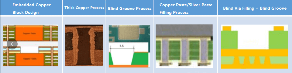
| Special Application Needs | Based on customer requirements, use special technologies or processes | Heat dissipation: Embedded copper block process, copper paste/silver paste plugging, laser hole filling… Durability for insertion/extraction: Gold fingers (enhance wear resistance and electrical connectivity for repeated plugging). These custom processes mitigate thermal and mechanical stresses in demanding environments. |
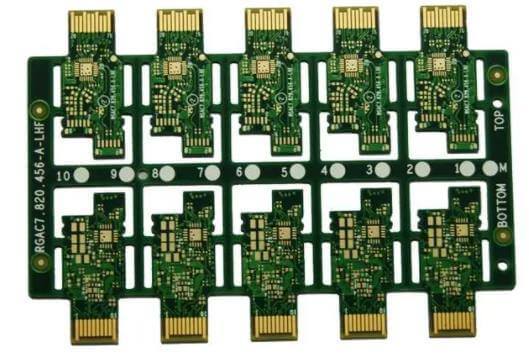
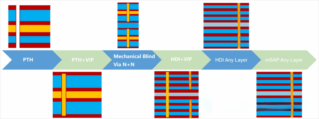
Common Optical Module PCB Designs
(Note: The original document features an image of common optical module PCB boards, sourced from the web. Visualize a diagram highlighting layered, high-density boards with gold fingers and vias.)
These designs exemplify the precision engineering required for optical communication products.
Typical Feature Areas of Optical Module PCBs
Optical module PCBs incorporate specialized regions to optimize performance:
- Dense Design: Due to size constraints and the need for high-speed data transmission, optical module PCBs employ multi-layering and blind via interconnections to boost routing density, accommodating multi-channel configurations.
- Heat Dissipation Design: As frequencies and bandwidths increase, heat generation rises, posing risks to reliability and signal integrity. Elevated temperatures can degrade performance, so advanced thermal management in optical module PCBs presents significant manufacturing challenges.
Key Technical Requirements for Optical Module PCBs
To address these demands, optical module PCBs must meet stringent specifications across several critical areas:
- Line Capabilities
- Line Width/Spacing (Width/Space): Evolving from traditional 100/100μm with ±20μm tolerance to 30/30μm with ±10μm tolerance, or even finer lines with tighter controls.
- Impedance Tolerance: From conventional ±10% to ±7%, and as low as ±5%.
- Alignment Capabilities
- Laser Via/Pad Diameter: Progressing from 100/250μm to 75/130μm, or down to 50/110μm.
- Solder Mask Ink Precision: Solder mask window-to-pad alignment from ±25μm to ±15μm, or smaller.
- Outline Precision
- Outline tolerance: ±0.1mm.
- Hole-to-hole center tolerance: From ±0.075mm to ±0.038mm.
- Pad-to-pad center tolerance: From ±0.075mm to ±0.05mm.
- PCB edge-to-gold finger tolerance: ±0.05mm.
- Slot diameter tolerance: ±0.05mm.
- Slot-to-gold finger tolerance: ±0.1mm.
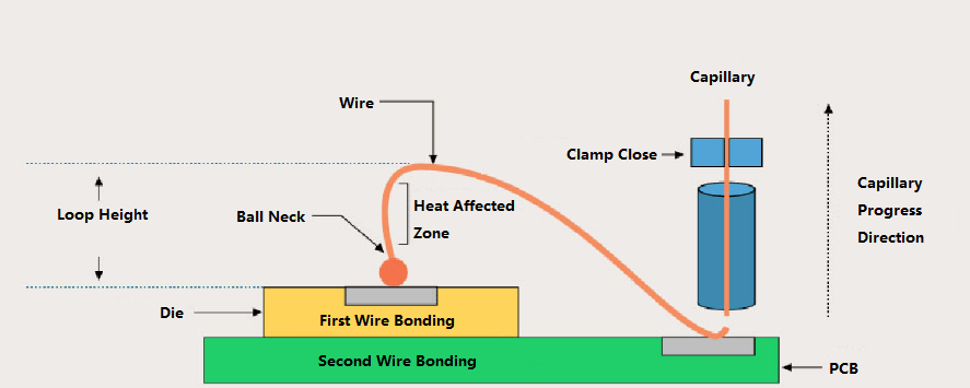
- Wire Bonding
- Wire Bonding Pad Size: 90/90μm, with ±15μm dimensional tolerance.
- Wire Pull Strength: ≥5g, requiring ball shear testing.
- Gold Fingers
- Appearance Standards: Strict requirements, such as no nickel exposure, protrusions, contamination, or scratches—specific to customer specs.
- Corrosion Resistance: Must pass customer-designated tests, like MFG testing.
- Durability for Insertion/Extraction: Endure at least 500 cycles per customer requirements.
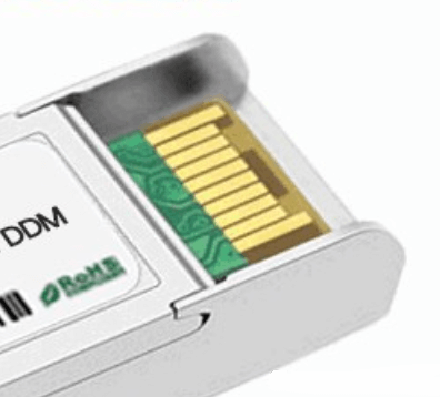
- Hot-Swappability: Graded/segmented gold fingers with no wire residue, meeting quality standards.
- Gold Finger Area Board Thickness: Tolerances are tightly controlled to customer needs.
- Embedded Copper Blocks
- Flatness: 0 to -10μm.
These technical demands highlight why partnering with experts in optical module PCBs is essential for cutting-edge applications.
Final Thoughts: Innovating for Tomorrow’s Networks
The interplay between optical modules and their PCBs is pivotal in sustaining the growth of AI-enabled networks. As demands for speed, efficiency, and reliability intensify, staying ahead requires innovative solutions that balance performance with cost.
FiberMall is a specialist provider of optical communication products and solutions, committed to delivering cost-effective offerings to global data centers, cloud computing environments, enterprise networks, access networks, and wireless systems. Renowned for its leadership in AI-enabled communication networks, FiberMall is an ideal partner if you’re seeking high-quality, value-driven optical modules and PCBs.
Related Products:
-
 NVIDIA MMA4Z00-NS Compatible 800Gb/s Twin-port OSFP 2x400G SR8 PAM4 850nm 100m DOM Dual MPO-12 MMF Optical Transceiver Module
$650.00
NVIDIA MMA4Z00-NS Compatible 800Gb/s Twin-port OSFP 2x400G SR8 PAM4 850nm 100m DOM Dual MPO-12 MMF Optical Transceiver Module
$650.00
-
NVIDIA MMA4Z00-NS-FLT Compatible 800Gb/s Twin-port OSFP 2x400G SR8 PAM4 850nm 100m DOM Dual MPO-12 MMF Optical Transceiver Module
$650.00
-
NVIDIA MMS4X00-NM Compatible 800Gb/s Twin-port OSFP 2x400G PAM4 1310nm 500m DOM Dual MTP/MPO-12 SMF Optical Transceiver Module
$900.00
-
NVIDIA MMS4X00-NM-FLT Compatible 800G Twin-port OSFP 2x400G Flat Top PAM4 1310nm 500m DOM Dual MTP/MPO-12 SMF Optical Transceiver Module
$1199.00
-
NVIDIA MMS4X50-NM Compatible OSFP 2x400G FR4 PAM4 1310nm 2km DOM Dual Duplex LC SMF Optical Transceiver Module
$1200.00
-
NVIDIA MMA4Z00-NS400 Compatible 400G OSFP SR4 Flat Top PAM4 850nm 30m on OM3/50m on OM4 MTP/MPO-12 Multimode FEC Optical Transceiver Module
$550.00
-
NVIDIA MMS4X00-NS400 Compatible 400G OSFP DR4 Flat Top PAM4 1310nm MTP/MPO-12 500m SMF FEC Optical Transceiver Module
$700.00
-
NVIDIA MMA1Z00-NS400 Compatible 400G QSFP112 VR4 PAM4 850nm 50m MTP/MPO-12 OM4 FEC Optical Transceiver Module
$550.00
-
NVIDIA MMS1Z00-NS400 Compatible 400G NDR QSFP112 DR4 PAM4 1310nm 500m MPO-12 with FEC Optical Transceiver Module
$700.00
-
OSFP-800G85F-MPO60M 800G OSFP SR8 MPO-12 Female Plug Pigtail 60m Immersion Liquid Cooling Optical Transceivers
$2400.00
-
OSFP-800G85M-MPO60M 800G OSFP SR8 MPO-12 Male Plug Pigtail 60m Immersion Liquid Cooling Optical Transceivers
$2400.00
-
OSFP-800G85F-MPO5M 800G OSFP SR8 MPO-12 Female Plug Pigtail 5m Immersion Liquid Cooling Optical Transceivers
$2330.00