
The maximum power consumption of 100G QSFP transceivers depends on the type and vendor of the transceiver. The table below summarizes the power consumption of Arista 100G QSFP transceivers.
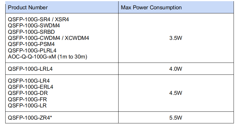
* The QSFP-100G-ZR4 is supported on specific platforms because of the higher power draw.
800G SR8 and 400G SR4 Optical Transceiver Modules Compatibility and Interconnection Test Report
Version Change Log Writer V0 Sample Test Cassie Test Purpose Test Objects:800G OSFP SR8/400G OSFP SR4/400G Q112 SR4. By conducting corresponding tests, the test parameters meet the relevant industry standards, and the test modules can be normally used for Nvidia (Mellanox) MQM9790 switch, Nvidia (Mellanox) ConnectX-7 network card and Nvidia (Mellanox) BlueField-3, laying a foundation for
Analysis of Management Methods for Unmanaged InfiniBand Switches
Why Unmanaged IB Switches Have No Web-UI 1) Positioning and Functional Simplification 2) Differences in Protocol Stack 3) Reducing Cost and Complexity How to Manage and Configure Unmanaged IB Switches Although there is no Web-UI, they can be managed via the following methods: 1) Connect to the Subnet Manager via
Analysis of Core Port Ratios in Intelligent Computing Center Network Design
Two Key Design Principles for GPU Cluster Networks The Definition of Core Ports In a typical Spine-Leaf (CLOS) network architecture for intelligent computing centers: Consistent Access-to-Core Port Ratios The number and bandwidth of “downlink ports” (used to connect servers) on a Leaf switch should maintain a fixed and sufficient ratio—typically 1:1
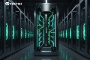
NVIDIA Spectrum-X Network Platform Architecture Whitepaper
Improving AI Performance and Efficiency AI workload demands are growing at an unprecedented rate, and the adoption of generative AI is skyrocketing. Every year, new AI factories are springing up. These facilities, dedicated to the development and operation of artificial intelligence technologies, are increasingly expanding into the domains of Cloud
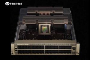
NVIDIA GB200 NVL72: Defining the New Benchmark for Rack-Scale AI Computing
The explosive growth of Large Language Models (LLM) and Mixture-of-Experts (MoE) architectures is fundamentally reshaping the underlying logic of computing infrastructure. As model parameters cross the trillion mark, traditional cluster architectures—centered on standalone servers connected by standard networking—are hitting physical and economic ceilings. In this context, NVIDIA’s GB200 NVL72 is

In-Depth Analysis Report on 800G Switches: Architectural Evolution, Market Landscape, and Future Outlook
Introduction: Reconstructing Network Infrastructure in the AI Era Paradigm Shift from Cloud Computing to AI Factories Global data center networks are undergoing the most profound transformation in the past decade. Previously, network architectures were primarily designed around cloud computing and internet application traffic patterns, dominated by “north-south” client-server models. However,
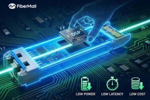
Why Is It Necessary to Remove the DSP Chip in LPO Optical Module Links?
If you follow the optical module industry, you will often hear the phrase “LPO needs to remove the DSP chip.” Why is this? To answer this question, we first need to clarify two core concepts: what LPO is and the role of DSP in optical modules. This will explain why