

The USFP connector is the electrical interface that connects a USFP optical module to the host system in a switch or SuperNIC. It uses a two-dimensional (2D) array connector with a two-step insertion design, in which high-speed contacts engage after the module is inserted.
The biggest challenge in scaling pluggable optics to 400 Gb/s per lane is not just the optical technology or DSP performance. The electrical connector is also a critical part of the design.
What Is the USFP Connector?
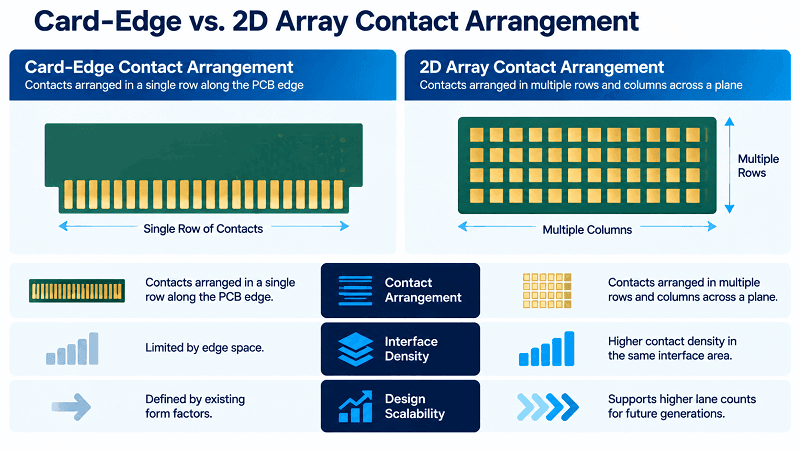
The USFP connector is the electrical interface between a USFP optical module and the host cage in a switch or network interface card. It uses a two-dimensional array of electrical contacts, meaning the contacts are arranged across a plane rather than in a single linear row. It also incorporates a two-step insertion mechanism designed to improve contact reliability and reduce wear.
Two clarifications up front, because the term invites confusion. First, “USFP” here stands for Ultra-Dense Small Form Factor Pluggable, the new form factor announced by NVIDIA and Cisco, not the older “uSFP” (Ultra Small Form-Factor Pluggable) used in some compact networking appliances. Second, this is a module-to-host electrical connector, not a fiber-optic connector like LC, SC, or MPO. The fiber interface, where optical signals enter and leave the module, is a separate connection entirely.
The connector is often an overlooked but critical component of any pluggable module. As per-lane signaling speeds and lane counts increase, the electrical interface faces more demanding requirements for signal integrity, contact reliability, and mechanical durability. This is one of the key reasons behind the new USFP connector architecture.
Why 400G-Per-Lane Signaling Needs a New Connector
The connector was redesigned because 400 Gb/s-per-lane electrical signaling places greater demands on three important aspects of connector design: signal integrity, contact reliability, and mechanical durability.
Signal Integrity: Crosstalk and Contact Resistance
At 400 Gb/s per electrical lane, maintaining signal integrity becomes increasingly challenging. A connector designed for eight electrical lanes at 200 Gb/s per lane cannot simply be assumed to support 16 lanes at 400 Gb/s per lane.
The design must carefully manage insertion loss, return loss, crosstalk, impedance discontinuities, and contact resistance. A higher-density contact arrangement also makes the electrical design more demanding.
The USFP 2D array architecture is intended to support more high-speed contacts while addressing the signal integrity requirements of next-generation electrical interfaces. However, the detailed contact pitch, grounding arrangement, and electrical performance specifications have not yet been publicly released.
Contact Wear and Mating Force
Connectors are subject to mechanical wear. Repeated insertion and removal can gradually affect contact surfaces and electrical reliability. At 400 Gb/s per lane, maintaining consistent contact performance becomes particularly important.
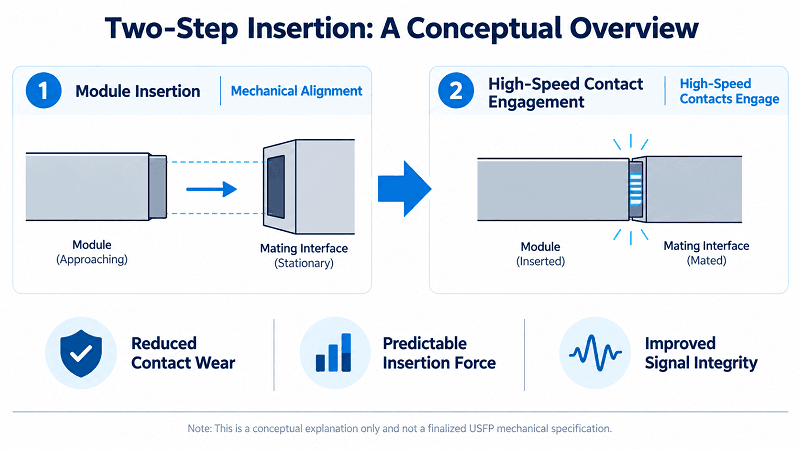
The USFP design addresses this challenge through its two-step insertion mechanism, which engages high-speed contacts after the module is inserted. This approach is intended to reduce unnecessary contact wear and make insertion force more predictable.
The Two-Dimensional (2D) Array Connector
The USFP connector arranges its electrical contacts in a two-dimensional array across the mating interface rather than relying on a single linear row. This architecture provides a different approach to increasing contact density in a pluggable optical module.
The 2D array offers three important design advantages:
- More contact positions. A two-dimensional arrangement provides additional contact positions across the available interface area, supporting a higher number of electrical connections.
- Support for higher lane density. The architecture is designed to accommodate the increased contact requirements of 400 Gb/s-per-lane interfaces while addressing signal integrity challenges.
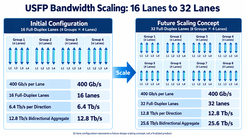
- Future scalability. The connector technology is designed to support an initial 16 full-duplex lanes, with a potential expansion to 32 or more lanes in future configurations.
That last point matters more than it sounds. A connector architecture with limited lane capacity can become a bottleneck as network bandwidth increases. By providing a path toward higher lane counts, the USFP design offers greater flexibility for future generations of pluggable optics.
It is important to note that the exact contact geometry, pitch, and electrical layout have not yet been published. Actual signal integrity performance will depend on the finalized connector design and qualification results.
Two-Step Insertion: How It Works and Why It Matters
The two-step insertion mechanism is one of the most distinctive features of the USFP connector. Unlike a conventional description of a simple plug-in connection, USFP uses a design in which high-speed contacts engage after the module is inserted.
At a high level, the mechanism separates module insertion from high-speed electrical contact engagement. The module is first inserted into the host interface, and the high-speed contacts engage after insertion.
The exact mechanical structure, contact geometry, and insertion-force profile have not yet been publicly disclosed. However, NVIDIA and Cisco have identified three key benefits of this design:
- Reduced contact wear. Delaying high-speed contact engagement is intended to reduce unnecessary mechanical wear during insertion and removal.
- More predictable insertion force. The two-step design is intended to make the insertion process more consistent and easier to manage during installation and maintenance.
- Improved signal integrity. Controlling when high-speed contacts engage helps support more reliable electrical connections at demanding signaling rates.
Consider a hyperscale operator’s regular maintenance window. Technicians may need to insert or replace optical modules across densely populated switch racks. Repeated module handling puts mechanical demands on connector interfaces.
A connector designed to reduce contact wear and make insertion force more predictable can help make these maintenance operations more consistent. For operators, this can contribute to better connector durability and more reliable service procedures.
The exact insertion sequence and mechanical behavior will depend on the finalized USFP hardware design and qualification results.
USFP Connector vs OSFP and QSFP-DD Connectors
How does the USFP connector compare with the connectors used in existing pluggable optical modules? The following table highlights the main differences.
| Comparison | QSFP-DD | OSFP | USFP |
| Electrical lanes | 8 Tx + 8 Rx | 8 Tx + 8 Rx | Initially 16 full-duplex lanes |
| Connector type | Card-edge, 76 contact pads | Card-edge, 60 contacts | 2D array connector |
| Contact engagement | Ground → Power → Signal | Ground → Power → Signal | Two-step insertion |
| Future scalability | Defined by the existing MSA | Defined by the existing MSA | Designed to scale to 32+ full-duplex lanes |
| Thermal design | Depends on module power class and host cooling | Depends on module power class and host cooling | Up to 100W power dissipation |
Note: QSFP-DD and OSFP use card-edge electrical interfaces with sequential contact mating: ground contacts engage first, followed by power and signal contacts. This is different from the USFP two-step insertion mechanism, which is specifically designed to engage high-speed contacts after module insertion.
The QSFP-DD specification defines 76 module contact pads, with 38 on each side of the paddle card. The OSFP specification defines a 60-contact edge connector.
The defining differences of USFP are its 2D array connector and two-step insertion design. Both are intended to support higher electrical lane density while maintaining signal integrity and the serviceability of pluggable optics.
For a broader comparison of the complete module form factors, see our USFP vs. OSFP vs. QSFP-DD comparison.
Thermal and Mechanical Design: The 100W Envelope
The connector does not operate in isolation. It must work reliably within the module’s overall thermal and mechanical design.
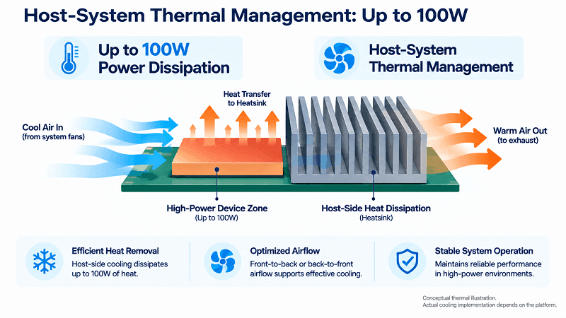
USFP is designed to support power dissipation of up to 100W without requiring a separate, dedicated embedded cooling circuit inside the transceiver. This is an important consideration for next-generation optical modules with higher power requirements.
At this power level, host-system thermal management becomes particularly important. The host platform must provide an appropriate thermal solution to maintain reliable module operation.
The specific thermal interface materials, heatsink configurations, airflow requirements, and cooling arrangements have not yet been fully disclosed. These details will depend on the final module and host-system implementations.
The 100W figure describes the announced power dissipation capability, not a requirement that every USFP module operate at 100W.
For a deeper look at the thermal considerations, see our USFP thermal design deep dive.
Who’s Building the USFP Connector?
USFP is not yet a finalized, published open industry specification. NVIDIA and Cisco have announced plans to develop an open industry specification through an upcoming community-led multi-source agreement (MSA) project.
The two companies are collaborating with TE Connectivity and Amphenol to develop USFP cages, connectors, and modules, with additional suppliers expected to join the ecosystem.
This multi-source approach is intended to establish a common hardware foundation for different manufacturers, encouraging broader industry participation and supporting a more flexible supply chain.
What the USFP Connector Means for Data Center Planning
Three questions should drive your own evaluation:
- How many insertions will the connector see? High-churn hyperscale racks benefit most from two-step insertion’s reduced contact wear.
- What’s your lane roadmap? If you’re planning past 1.6T toward 3.2T, a connector with 32-lane headroom is insurance.
- Is it field-serviceable? The 2D array and two-step seating are designed to keep modules pluggable and replaceable, unlike co-packaged optics.
One honest caveat before you commit anything to a roadmap. USFP is a specification, not a shipping product. The 2D array dimensions, contact pitch, lane mapping, and qualification methods have not been published yet.
The 4× density and 1.3× efficiency figures are design targets on a proposed standard. Treat the connector as a signal of where pluggable optics are heading, not a part you can order tomorrow.
FiberMall is tracking USFP as the form factor matures. In the meantime, our 400G and 800G optical transceivers and DAC/AOC cables cover the AI-fabric interconnects you can deploy today.
Conclusion
The USFP connector uses a 2D array architecture and two-step insertion design to support next-generation pluggable optical modules operating at 400 Gb/s per electrical lane. High-speed contacts engage after the module is inserted, an approach intended to reduce contact wear, improve signal integrity, and make insertion force more predictable.
The design matters because it provides a path toward higher electrical lane density and greater bandwidth capacity. The initial planned configuration supports 16 full-duplex lanes, delivering 6.4 Tb/s in each direction, or 12.8 Tb/s of aggregate bidirectional capacity. The connector technology is also designed to scale to 32 or more full-duplex lanes in future configurations.
Combined with an OSFP-sized footprint and support for up to 100W of power dissipation, USFP represents an important development in the evolution of pluggable optics for AI networks.
For network engineers and data center architects, the takeaway is simple: the connector is no longer a component that can be overlooked. It plays an increasingly important role in determining how far pluggable optical interfaces can scale while maintaining signal integrity, reliability, and serviceability.
USFP is not shipping yet, but its announced design direction highlights how the next generation of high-density optical interconnects may evolve.