The 400G QSFP-DD transceiver module is the mainstream package specification for 400G customer interfaces. The following article will share the key factors for successful testing, troubleshooting, and verification of QSFP-DD modules for optical network designers, network component manufacturers, and end users.
Customer interface speeds are steadily increasing, with typical rates increasing at least ten times every decade. 100GE has been widely deployed through the QSFP28 interface, and we are in the early stages of 400G deployment. IEEE1 developed the 400G Ethernet client interface standard as part of the 802.3.bs, which was officially standardized in December 2017. Early adopters are using the CFP-8 package specification, but the broader market is focused on QSFP-DD, which allows for a degree of backward compatibility with the widely adopted QSFP28.
Because Ethernet has a wide range of applications and is available with a range of PMD (physical medium dependent), it allows a single “QSFP-DD” slot to support a large number of applications, ranging from several meters of passive copper-cable DAC cable to 80 km of coherent ZR. There are also a few companies that focus on OSFP packaging specifications. While not as extensive and backward compatible, it does offer some advantages in terms of electrical signal integrity and thermal management. Most of what follows about QSFP-DD applies to OSFP and the VIAVI ONT family, which supports many applications based on OSFP.
400G relies on high-order (PAM-4) modulation for both the electrical module-to-host interface and the electrical or optical PMD. PAM-4 modulation is used to maximize data capacity for a given bandwidth, but it presents significant challenges in terms of complexity and performance, which also means that the link requires forward error correction (FEC) coding to implement reliable data transmission.
Why Choose QSFP-DD?
100G Ethernet was deployed in 2008 with early designs based on CFP pluggable modules. The second generation of systems migrated to CFP2 (or CPAK from a major equipment manufacturer) and then chose QSFP28, which drove widespread and cost-effective volume adoption. CFP4 was an earlier challenge for QSFP28, but QSFP28 drove significant 100G growth due to many factors. The industry is mindful of the importance of packaging specifications and wants to minimize the additional complexity and cost challenges associated with the multi-step evolution of 400G packaging specifications. CFP8 allows beginning adopters to develop and validate 400G. However, it did not meet the requirements of density, power, cost, and “compatibility”, so the industry quickly adopted QSFP-DD as the target. And someone come up with an alternative, OSFP, which provides excellent technical solutions, but did not meet the urgent need for interface support of traditional legacy transceivers. In principle, the QSFP-DD optical port could support the traditional QSFP-28 optical module – this would allow switch manufacturers to ship 400G devices that could be shipped along with 100G modules, and the on-site upgrade would be a simple module replacement.
Some enhancements have been made to the existing QSFP28 to meet the higher bandwidth, power, and cooling demands of the move to 400G. These enhancements include a doubling of the high-speed electrical port channel (from a 4-channel 25 Gbps NRZ enhancement to an 8-channel 56 Gbps PAM-4) and an extension of the “front end” of the module to provide greater internal volume and enhanced thermal performance. In addition, further work was carried out to enhance the module control interface leading to the CMIS 4.05 standard.
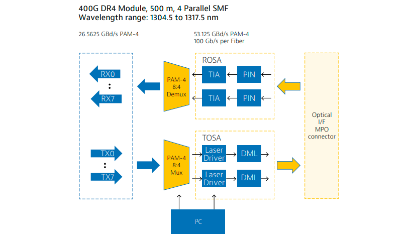
The 400G QSFP-DD DR4 is one of the most common 400G customer optical interfaces deployed in 2020. It transmits 400G in the form of four 100G signals over separate single-mode fibers. It has a wide range of applications in enterprises. It supports 500 m coverage and is able to connect to a separate 100G Ethernet link, making it attractive as a high-density 100G solution, which can quadruple the port count density.
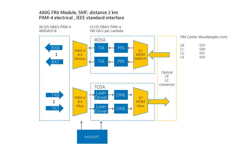
The 400G QSFP-DD FR4 interface will also have a wide range of applications, including telecommunications. It provides a 2km longer link budget via a single-mode optical fiber. The 400G is carried by four 100G signals, each with a slightly different wavelength.
400G PMD Modules (Physical Medium Dependent)
| PMD | Reach | Application | Technology |
|---|---|---|---|
| DAC | 2 to 3 m | Intra-rack & server | Passive copper cable, 50G PAM-4 electrical |
| SR8 | 100 m | Enterprise | Parallel multi-mode, 50G/λ – PAM-4 |
| DR4 | 500 m | Datacenter and enterprise | Parallel single-mode, 100G/λ – PAM-4 |
| FR4 | 2 km | Large scale datacenter | Single-mode, 100G/λ, PAM-4 |
| LR8 | 10 km | Telecom reach | Single-mode, 100G/λ, PAM-4 |
| ZR | 80 km | Metro and DCI | Single-mode/coherent, PAM-4 |
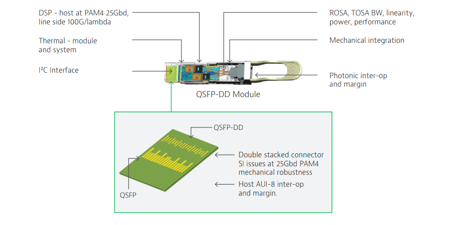
Standards and Themes of QSFP-DD
Many standards and MSA are applicable. It is also important to understand the critical tests for each phase of the development cycle, from basic IC evaluation through module hardware integration, software, and firmware, to vendor selection and acceptance. The production also has its own set of critical test requirements.
A solid understanding of key documents such as IEEE, CMIS, QSFP-DD, MSA, and OIF is required to successfully design, test, verify, manufacture, and deploy pluggable optical modules and devices. QSFP-DD is the perfect combination of electronics, optics, mechanics, thermal management, and firmware integration. All components must work together before the module can be successfully deployed.
Interoperability
The great advantage of the Ethernet customer interface ecosystem is that we have a strong and clear set of standards driven by IEEE and other standards that allow multi-vendor ecosystems to interoperate without resorting to “engineered” links.
Both the module-to-host interface and the module-to-fiber interface are key to this interoperability. On the host-to-module interface, we focus on three main areas:
- High-speed data paths (AUI) built from chip to module (C2M) face multiple challenges, including signal integrity and signal balancing. While a portion of the FEC budget is allocated to this part of the link, any problems with this interface can cause significant problems with the link. Poorly “tuned” links (in terms of equalizers and channels) can lead to intractable problems, such as random bursts or the worst case accidental bit slippage.
- Module Management – This I²C interface based has evolved from the basic memory mapping management of SFF-8636 to the 100G QSFP28 to the complex state complete CMIS 4.0. This evolution is extremely challenging for the ecosystem, and a solid working knowledge of CMIS 4.0 documentation is key to robust and stable module management.
- Module power – For pluggable coherent (QSFP-DD ZR) modules for DCI applications, module power requirements have climbed from a few watts at 100G to possibly close to 20W. This puts forward high requirements for the robustness and stability of the power supply. In addition, it must be able to provide dynamic and transient characteristics of power demand when the module is awakened.
These areas are all closely intertwined and need to be treated as a whole (especially in the context of CMIS 4.0 module management) to ensure that modules are operating without failure.
PAM-4
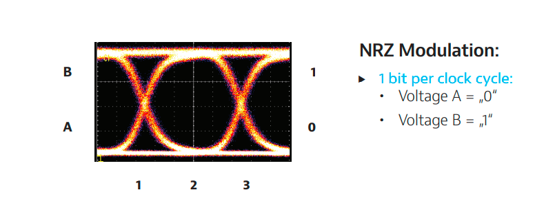
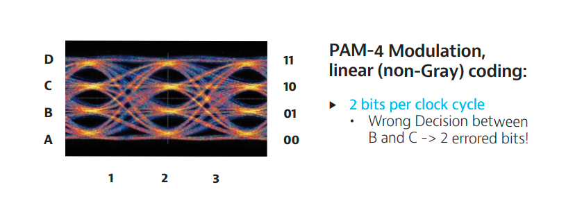
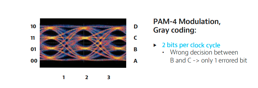
Both electrical (module to host interface) and optical (electrical) links are PAM-4 modulated. This higher-order modulation scheme allows doubling the number of bits sent per unit of time. While NRZ technology is widely used and mature for high speeds, SERDES PAM-4 is a relatively new technology that is more complex and challenging. We have extensive experience in the bit error analysis of NRZ links. But we still see problems with the 10G to 25G NRZ channel used at 100GE. Therefore, the shift to PAM-4 is expected to be a significant challenge for the entire industry. This is further complicated by the use of FEC-based links, which always have background BER and much more complex channel equalization. To be fair, PAM-4 is an order of magnitude more complex than the widely used 25G NRZ.
FEC
Because it was challenging to develop a component that could provide error-free PAM-4 transmissions, the developers used an FEC that could protect both the electrical module interface and the optical module-to-module interface. We put a lot of effort into a careful understanding of the bit error mechanism in the transmission channel and components, and how the “cost” of FEC logic (encoding and receiving) is balanced. The “cost” of FEC includes additional circuits that consume power and can increase the delay of any link.
DSP and Equalizer
At 400G, it was decided to use the concept of a “powerful” electrical reception equalizer to face the “worst case” transmitter and “worst case” channel performance. This can lead to the closure of the PAM-4 eye pattern at the input of the PAM-4 receiver, so the PAM-4 receiver requires a powerful and possibly complex receiver to balance transmit and channel effects in order to recover a clear eye pattern to achieve correct decoding of a given symbol. The complexity of the equalizer means that in most cases DSP-based solutions have to be implemented, which can have an impact on power, delay, complexity, bit error performance, and management or control. While DSP equalizers are powerful, the complexity of their functionality can lead to challenges such as finding the best Settings for taps. In addition, the equalizer is often hidden behind the DSP firmware and control API, making it highly abstract to the user. The measurement of TDECQ6 presents additional challenges – this measurement is complex and may not be consistent, which further increases the challenge of a freely interoperable, multi-vendor ecosystem.
Key Points
There will always be bit errors – links now always have background bit error rates. The “fingerprint” of bit error statistics is crucial. True random BER streams are usually compatible with the FEC used to protect the link. But bursts, slips, and other deterministic issues can severely degrade the FEC’s error correction capability. In a real link, BER can be a complex mix of electrical and optical channel noise, crosstalk, signal integrity issues, bursts, bit slips, and even BER proliferation due to incorrectly set equalizers.
What ultimately matters is how the FEC performs when given a specific BER fingerprint. What is the margin? How long will it be before we receive dropped packets? Can we predict long-term performance to understand link degradation? What are the root causes of BER?
Several tools can be used to investigate BER characteristics, from error bias in individual PAM-4 code elements to bit-slip nature burst analysis. The understanding of BER bias can be further enhanced by tools such as clock variation and skew.
PAM-4 symbol analysis can be used to ensure that there is no “level” bias in the bit error distribution. The stability of key photonic elements (such as the receiver photonic AGC) can be further verified by observing the variation in the time power of the PAM-4-bit error distribution (via an attenuator).
It is important to fully investigate the bit error bursts and confirm that they are bursts and not bit (or symbol) slippage. Slippage is usually associated with the DSP (and associated firmware) and cannot be corrected by FEC. General tests cannot distinguish between burst problems caused by classical signal integrity or noise issues and burst problems related to clock and phase sensitivity. As a result, a number of new tools and techniques must be deployed to investigate the nature and root cause of QSFP-DD bit errors.
The simplest top-level view can be obtained by looking at the number of 10-bit code element errors per 5440 bit FEC codeword (KP4 FEC). We would normally expect a monotonically distributed count per symbol to drop by about 10. That is, for every additional incorrect symbol/codeword, we expect the number of errors to decrease by 10. Any long tails or isolated spikes are indicative of some non-random (systematic) cause. We also expect the number of error symbols to increase by a factor of 10 in the measurement time. Thus, if we observe a count of 10 error symbols per codeword after 10 seconds, we expect to see 11 error symbol counts after about 100 seconds.
Such a rule of thumb can be used to estimate the time to an uncorrectable error (16 or more errors per codeword). For example, after 100 hours of testing time, if we observe at most 12 error symbols/codewords, we would expect the following approximation:
| Errored symbols | Time | Notes |
|---|---|---|
| 12 | 100 hours | Measurement |
| 13 | 1000 hours | Estimate |
| 14 | ~420 days | |
| 15 | ~11 ½ years | |
| 16 (uncorrectable error) | ~114 years | First dropped packet after > century |
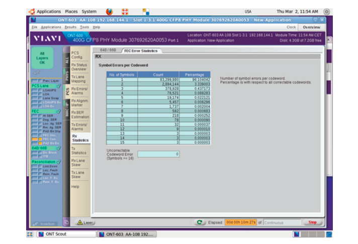
FEC – Error symbol/codeword
In the case below, ONT operates using a severely attenuated 400G fiber link such that significant bit errors occur within a 10-min interval. This is what can be expected from a compliant link. As you can see, the distribution is generally monotonic. The count per error symbol drops, but it does show a slightly longer tail than 12 error symbols/codeword. In this case, the link is likely to drop the packet due to an uncorrected codeword.
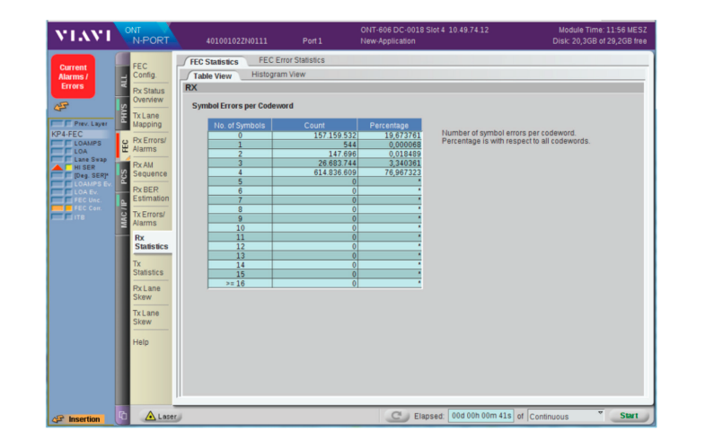
The screenshot below shows a situation where a serious problem occurs. Although FEC has a large margin (we can see up to four error symbols in a codeword), the distribution is not monotonic, suggesting a potential source of bit errors in this system. Note that this 100G link example was generated by a special VIAVI ONT application that creates extensive FEC error distributions for stress testing and verification of FEC logic and power integrity.
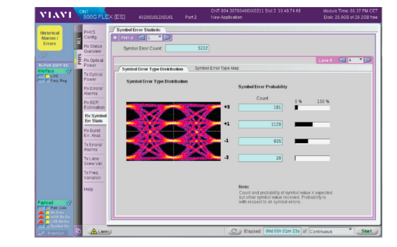
ONT can not only analyze the bit error distribution and code type on the whole sequence but also track the bit error characteristics on the basis of each PAM-4 symbol.
A dynamic skew variation is a powerful tool for stress testing and verification of the QSFP-DD module. It can be used to verify compliance with IEEE802.3 standards and the overall stability of the DSP and associated firmware. This is especially important in the DR4 module, where a pair of individual electrical and optical channels may be located in completely different clock domains!
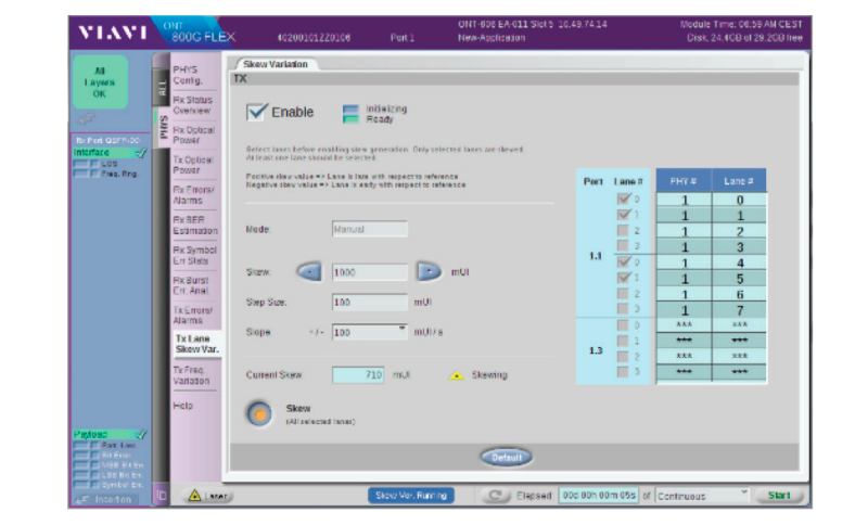
The screenshot above shows the dynamic skew application of PAM-4. It is able to precisely control the relative timing of the transport channel with respect to the UI while still maintaining “uninterrupted” phase shifts, which is key to solving challenging issues such as crosstalk and DSP-based firmware timing issues.
Dynamic skew (or skew variation) is a key test for any parallel channel communication system. It can be used for signal integrity testing and verification (crosstalk) and also for stress testing and verification of FIFO and CDR performance in PAM-4 SERDES.
Different degrees of skew can also be used to investigate signal integrity and crosstalk issues, which have a wide range of applications in hardware and SI teams. The channel timing can be adjusted to ensure that the interference source channel transition occurs in the middle of the PAM-4 eye pattern of the interfered object channel.
PAM-4 signals (because of the low signal margin) are more susceptible to crosstalk than classical NRZ. In the dense range of the QSFP-DD (especially around the host connector), the high-speed PAM-4 channels are wired very close together and care must be taken to avoid signal crosstalk problems. Normally, the BER tester runs parallel channels at a fixed phase, so “worst-case alignment” may not occur under SI stress testing. With dynamic skew, the source channel can be scanned in relative phase to fully verify that problems do not occur, even in the worst-case phase shift scenario. The end user only needs to observe if there is an error at a specific phase offset (usually when the source channel has a level transition in the middle of the “eye diagram” of the interfered object).
Modern SERDES uses a series of FIFO buffers to retime and realign the signal before further processing within the IC structure. The realignment uses a series of FIFO buffers that recover the clock from the main clock source (usually the main channel through the CDR).
If the system is not designed or implemented correctly, it is possible that phase variations and changes between the primary channel (CDR reference channel) and other channels are causing the FIFO to be unaligned or even sliding. This will manifest itself as a bit-slip, which the ONT advanced error analysis can track as a bit-slip, rather than as a burst error as seen with traditional test equipment. Using the dynamic skew application, ONT can intentionally stress test the performance of the CDR/FIFO in SERDES and attempt to force a failure mode through skew (range and rate). This, combined with ONT’s advanced BER analysis, provides a very powerful and complete test system for SERDES testing and can be used to quickly solve very challenging problems in 400GE links that occasionally cause bit slippage. ONT PAM-4 dynamic skews can force the generation of these BERs to help diagnose and resolve the root cause.
General 400G QSFP-DD Control Screen
Module management has evolved over time from the very basic register-based system SFF 8636 to CMIS 4.0, which is a comprehensive management system with complete module status designed to meet the needs of more complex modules 400GE and up.
The close interaction between modules through I²C control interfaces, power and control pins, and data paths is essential for robust and stable operation of modules. Module complexity is higher, especially for data path balancing in module DSP, which requires a more comprehensive understanding of the control setup and execution between host and module. Under CMIS 4.0, commands, operations, and timing behaviors must be tightly choreographed in the correct order. If you’re not careful, one module may appear to run fine in one host slot, but another (with subtle differences in timing around commands, power, and data paths) may run erratically. Or worse, the bit error rate increases and a rare and intractable problem occurs most likely bit slippage. Tools such as ONT integrate CMIS commands on I²C, as well as module power control and data path status, which not only help to debug and solve problems but also help to stress test and verify the robustness of modules in different hosts.
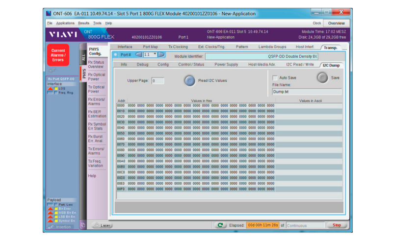
The screen above shows a memory dump of the first page of memory. This allows you to quickly check that the correct values are stored in the 400G QSFP-DD EEPROM. Blank or random data may indicate that the device has not been initialized.
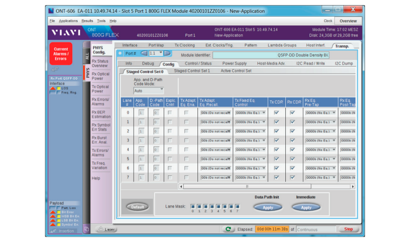
Some of the more advanced applications in the module management application allow precise control of the module’s electrical port parameters in a clear and unambiguous manner.
In summary
400G QSFP-DD modules are a marvel of electronic, photonic, mechanical, and thermal engineering combined with complex firmware. A healthy multi-vendor QSFP-DD ecosystem is critical to the widespread deployment of 400G networking technology. It represents an evolution and revolution in traditional 100G module technology but also brings new challenges, including PAM-4 signalings (electrical and optical), FEC for link BER control, and the new complexities of CMIS 4.0.
These challenges are greater because the scale and deployment needs of hyperscale users are driving changes in pricing expectations. Production must meet yield and throughput requirements to meet price expectations, while also having the coverage and analysis capabilities to meet the new challenges of PAM-4.
Related Products:
-
 QSFP-DD-400G-SR8 400G QSFP-DD SR8 PAM4 850nm 100m MTP/MPO OM3 FEC Optical Transceiver Module
$149.00
QSFP-DD-400G-SR8 400G QSFP-DD SR8 PAM4 850nm 100m MTP/MPO OM3 FEC Optical Transceiver Module
$149.00
-
QSFP-DD-400G-DR4 400G QSFP-DD DR4 PAM4 1310nm 500m MTP/MPO SMF FEC Optical Transceiver Module
$400.00
-
QSFP-DD-400G-XDR4 400G QSFP-DD XDR4 PAM4 1310nm 2km MTP/MPO-12 SMF FEC Optical Transceiver Module
$580.00
-
QSFP-DD-400G-FR4 400G QSFP-DD FR4 PAM4 CWDM4 2km LC SMF FEC Optical Transceiver Module
$500.00
-
QSFP-DD-400G-LR4 400G QSFP-DD LR4 PAM4 CWDM4 10km LC SMF FEC Optical Transceiver Module
$600.00
-
QSFP-DD-400G-PLR4 400G QSFP-DD PLR4 PAM4 1310nm 10km MTP/MPO-12 SMF FEC Optical Transceiver Module
$1000.00
-
QSFP-DD-400G-ER4 400G QSFP-DD ER4 PAM4 LWDM4 40km LC SMF without FEC Optical Transceiver Module
$3500.00
-
QSFP-DD-400G-LR8 400G QSFP-DD LR8 PAM4 LWDM8 10km LC SMF FEC Optical Transceiver Module
$2500.00
-
QSFP-DD-400G-ER8 400G QSFP-DD ER8 PAM4 LWDM8 40km LC SMF FEC Optical Transceiver Module
$3800.00
-
QSFP-DD-400G-DCO-ZR 400G Coherent QSFP-DD DCO C-band Tunable Optical Transceiver Module
$6000.00