Nvidia’s GPU interconnect technology has two main types of memory slots: PCIe and SXM. These two interfaces have different functions and performance.
PCIe interface is a widely used general protocol. Although it has comprehensive functions, it has a relatively slow transmission speed for GPU interconnect. Nevertheless, PCIe interface GPU cards can still communicate with CPU and other GPU cards in the server through PCIe slots. In addition, they can also exchange data with devices on external server nodes through network cards. If users want to improve the transmission speed of PCIe GPU cards, they can use NVLink bridge to achieve fast communication between GPU and CPU. However, it should be noted that this method usually only supports the connection between two GPU cards. That is to say, PCIe GPU cards usually need to appear in pairs, connected by NVLink Bridge, and transmit data through PCIe channel. It is worth noting that the latest PCIe standard has a limit of 128GB/s in network bandwidth.
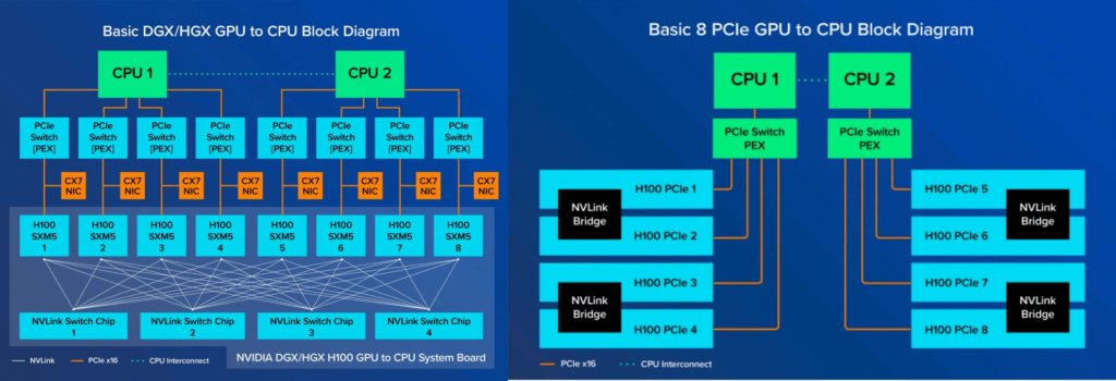
In contrast, the SXM interface is designed specifically for high-performance GPU interconnection. It uses a dedicated protocol laid out on the circuit board, which enables SXM to offer higher transmission speed and better native NVLink support than PCIe in terms of inter-card connection. Its memory bandwidth is also superior to PCIe. SXM architecture is especially suitable for connecting GPUs to NVIDIA’s proprietary DGX and HGX systems. In these systems, SXM-based GPUs are connected through NVSwitch integrated on the motherboard, without relying on PCIe for communication. This design allows SXM to support up to 8 GPUs interlinked, achieving very high bandwidth. For example, the uncut A100 and H100 can reach 600GB/s and 900GB/s of bandwidth respectively, while the slightly cut A800 and H800 can reach 400GB/s of bandwidth.
Users should generally weigh the pros and cons of PCIe-based or SXM-based GPUs according to their specific application scenarios and performance requirements.
PCIe (PCI Express) Introduction
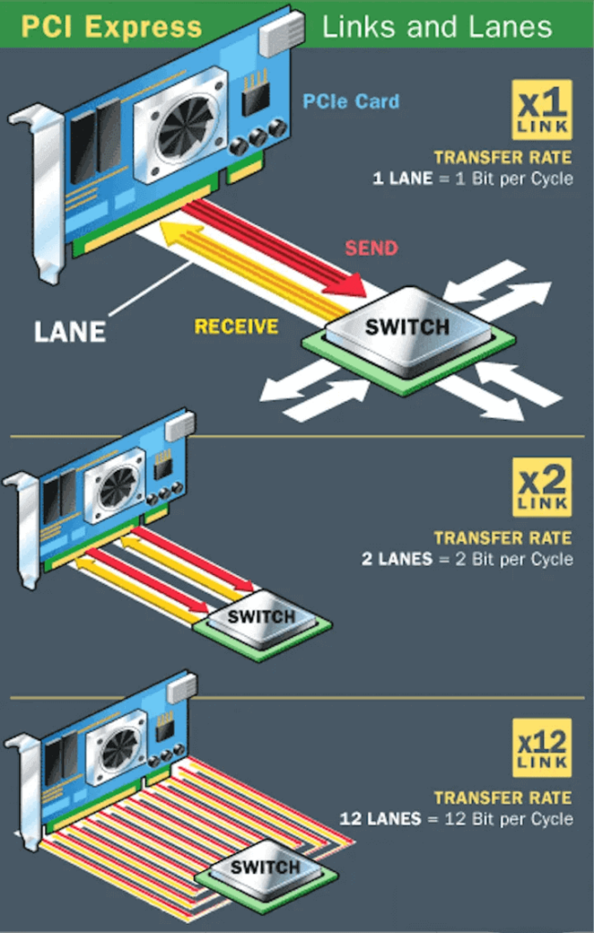
PCIe, short for PCI Express, is an advanced computer expansion bus standard, whose core goal is to improve data throughput and communication speed between devices. As a full-duplex connection bus, the data transfer rate of PCIe depends on its number of lanes. Each lane consists of two pairs of data lines (one for sending, one for receiving), and each pair of data lines contains two differential lines. For example, X1 means one lane and four data lines, which can transfer 1bit data per direction per clock cycle; while X2 means two lanes and eight data lines, which can transfer 2bit data per cycle. Similarly, there are also X12, X16, X32 and other configurations.
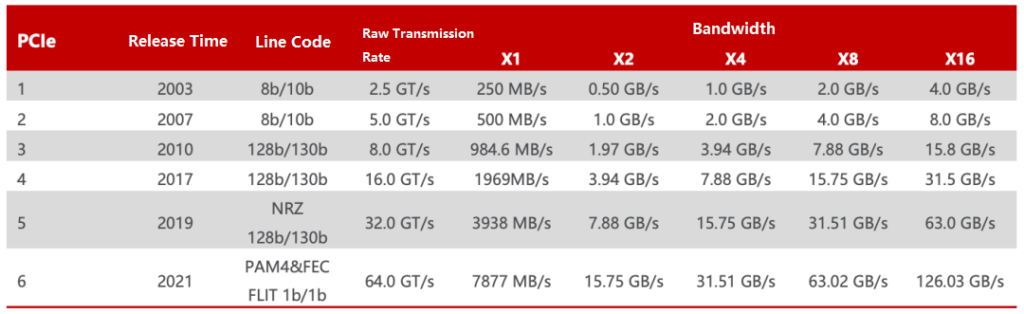
Since the release of PCIe 1.0 in 2003, its transmission rate has been increasing steadily. PCIe 1.0 supports a transmission rate of 250 MB/s per channel, with a total transmission rate of 2.5 GT/s. By 2007, the PCIe 2.0 specification doubled the total transmission rate to 5 GT/s, and the transmission rate per channel also increased to 500 MB/s. By 2022, the PCIe 6.0 specification further increased the total transmission rate to 64 GT/s. In June of the same year, the PCI-SIG alliance announced the PCIe 7.0 specification, which is expected to achieve a single-channel (x1) unidirectional transmission rate of 128 GT/s in the final version to be released in 2025.
PCIe Throughput Calculation
When calculating PCIe throughput (or available bandwidth), two factors need to be considered: transmission rate and encoding scheme. The transmission rate is usually expressed in GT/s (Giga Transitions per second), which describes the speed attribute of the physical layer communication protocol, rather than the number of bits transmitted per second (Gbps). This is because the transmission rate includes overhead bits that do not provide additional throughput. For example, PCIe 1.x and PCIe 2.x use the 8b/10b encoding scheme, which means that 20% of the original channel bandwidth is used for overhead.
Therefore, although the PCIe 2.0 protocol supports a transmission rate of 5.0 GT/s, due to the use of the 8b/10b encoding solution, the actual effective rate of each lane is 5*8/10=4 Gbps, or 500 MB/s. Similarly, the PCIe 3.0 protocol supports a transmission rate of 8.0 GT/s, but after using the 128b/130b encoding scheme, the actual effective rate of each lane is about 7.877 Gbps, or 984.6 MB/s.
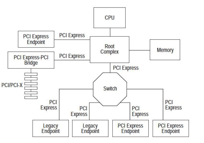
PCIe architecture consists of PCIe devices of different types, such as Root Complex (RC), Switch, and Endpoint (EP). Among them, RC is the only one in the bus architecture, responsible for connecting the processor and memory subsystems with the I/O devices. The function of the Switch is usually implemented by software, containing two or more logical PCI-to-PCI bridges (PCI-PCI Bridge) to ensure compatibility with existing PCI devices. This architecture provides strong support for high-performance computing and communication.
NVLink: A high-speed interconnect technology to accelerate GPU communication
As the computing power continues to increase, multi-GPU cards become the key to improving performance. However, the traditional PCIe bus is prone to be a bottleneck in data transfer rate and latency, limiting the efficiency and performance of GPU parallel computing.
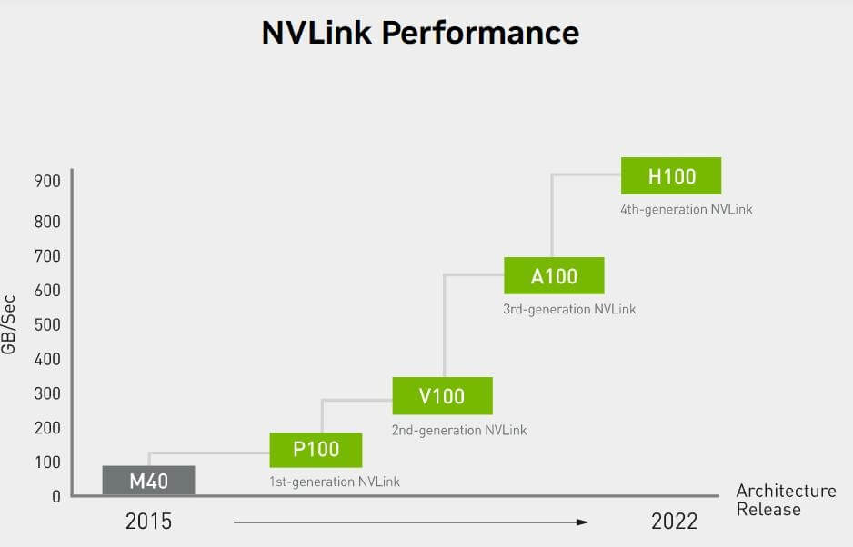
To solve this problem, NVIDIA introduced GPUDirect P2P technology, which allows GPUs to directly access the memory of other GPUs through PCI Express, reducing the latency of data exchange. But even so, due to the PCI Express bus protocol and topology limitations, it still cannot meet the higher bandwidth requirements. For this reason, NVIDIA further launched NVLink high-speed interconnect technology. NVLink aims to speed up the data transfer between CPU and GPU, and GPU and GPU, providing a more efficient and low-latency interconnect solution. Since its first release in 2014, NVLink has been continuously upgraded, and the bandwidth has been increasing. From P100’s 160GB/s to V100’s 300GB/s, and then to A100’s 600GB/s, NVLink’s bandwidth has been increasing, providing strong support for high-performance computing.
NVLink high-speed interconnect has two main implementation methods: one is through a bridge, and the other is to integrate NVLink interface on the motherboard. Both methods can achieve high-speed interconnection between GPUs and improve system performance.
NVSwitch: Seamless, High-Bandwidth Multi-GPU Communication
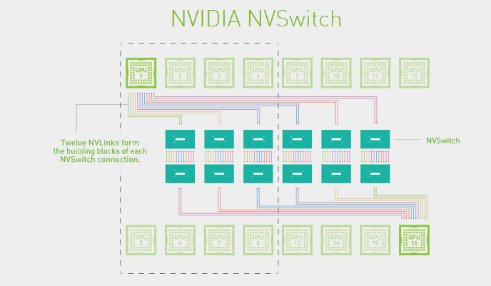
To solve the problem of imbalanced communication among GPUs, NVIDIA introduced the NVSwitch chip. NVSwitch is a physical chip (ASIC) similar to a switch, which can connect multiple GPUs at high speed through the NVLink interface. It can create a seamless, high-bandwidth multi-node GPU cluster, enabling all GPUs to work together in a cluster with full-bandwidth connectivity, thereby improving the communication efficiency and bandwidth among multiple GPUs within the server.
The combination of NVLink and NVSwitch enables NVIDIA to efficiently scale AI performance to multiple GPUs, providing powerful support for high-performance computing and artificial intelligence applications. Since the release of the first generation of NVSwitch in 2018, NVSwitch has evolved to the third generation. The third generation of NVSwitch is built with TSMC’s 4N process, and each chip has 64 NVLink 4.0 ports, with a communication rate of up to 900GB/s between GPUs. This innovative technology provides a broader development space for future high-performance computing and artificial intelligence applications.
Related Products:
-
 NVIDIA MMA4Z00-NS400 Compatible 400G OSFP SR4 Flat Top PAM4 850nm 30m on OM3/50m on OM4 MTP/MPO-12 Multimode FEC Optical Transceiver Module
$550.00
NVIDIA MMA4Z00-NS400 Compatible 400G OSFP SR4 Flat Top PAM4 850nm 30m on OM3/50m on OM4 MTP/MPO-12 Multimode FEC Optical Transceiver Module
$550.00
-
NVIDIA MMA4Z00-NS-FLT Compatible 800Gb/s Twin-port OSFP 2x400G SR8 PAM4 850nm 100m DOM Dual MPO-12 MMF Optical Transceiver Module
$650.00
-
NVIDIA MMA4Z00-NS Compatible 800Gb/s Twin-port OSFP 2x400G SR8 PAM4 850nm 100m DOM Dual MPO-12 MMF Optical Transceiver Module
$650.00
-
NVIDIA MMS4X00-NM Compatible 800Gb/s Twin-port OSFP 2x400G PAM4 1310nm 500m DOM Dual MTP/MPO-12 SMF Optical Transceiver Module
$900.00
-
NVIDIA MMS4X00-NM-FLT Compatible 800G Twin-port OSFP 2x400G Flat Top PAM4 1310nm 500m DOM Dual MTP/MPO-12 SMF Optical Transceiver Module
$1199.00
-
NVIDIA MMS4X00-NS400 Compatible 400G OSFP DR4 Flat Top PAM4 1310nm MTP/MPO-12 500m SMF FEC Optical Transceiver Module
$700.00
-
NVIDIA(Mellanox) MMA1T00-HS Compatible 200G Infiniband HDR QSFP56 SR4 850nm 100m MPO-12 APC OM3/OM4 FEC PAM4 Optical Transceiver Module
$139.00
-
NVIDIA MFP7E10-N010 Compatible 10m (33ft) 8 Fibers Low Insertion Loss Female to Female MPO Trunk Cable Polarity B APC to APC LSZH Multimode OM3 50/125
$47.00
-
NVIDIA MCP7Y00-N003-FLT Compatible 3m (10ft) 800G Twin-port OSFP to 2x400G Flat Top OSFP InfiniBand NDR Breakout DAC
$260.00
-
NVIDIA MCP7Y70-H002 Compatible 2m (7ft) 400G Twin-port 2x200G OSFP to 4x100G QSFP56 Passive Breakout Direct Attach Copper Cable
$155.00
-
NVIDIA MCA4J80-N003-FTF Compatible 3m (10ft) 800G Twin-port 2x400G OSFP to 2x400G OSFP InfiniBand NDR Active Copper Cable, Flat top on one end and Finned top on other
$600.00
-
NVIDIA MCP7Y10-N002 Compatible 2m (7ft) 800G InfiniBand NDR Twin-port OSFP to 2x400G QSFP112 Breakout DAC
$190.00