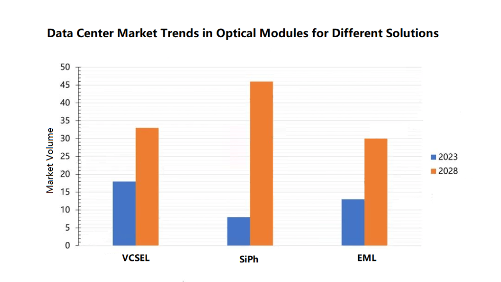
In the high-speed Ethernet modules operating at 400G, 800G, and 1.6T, the market for VCSEL, EML, and silicon photonics is expected to grow.
The overall RF bandwidth needs to be considered for high-speed VCSELs, which are currently used in 100G PAM4 channels, 4x100G 400G modules, and 8x100G 800G modules. The bandwidth impact goes beyond just the chip design level, as the packaging aspect also plays a crucial role.
Similarly, the industry is also closely examining the bandwidth impact of EML packaging.
The PN junction capacitance is an important aspect in the chip design of VCSELs and EMLs that affect bandwidth.
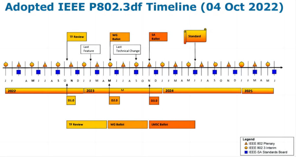
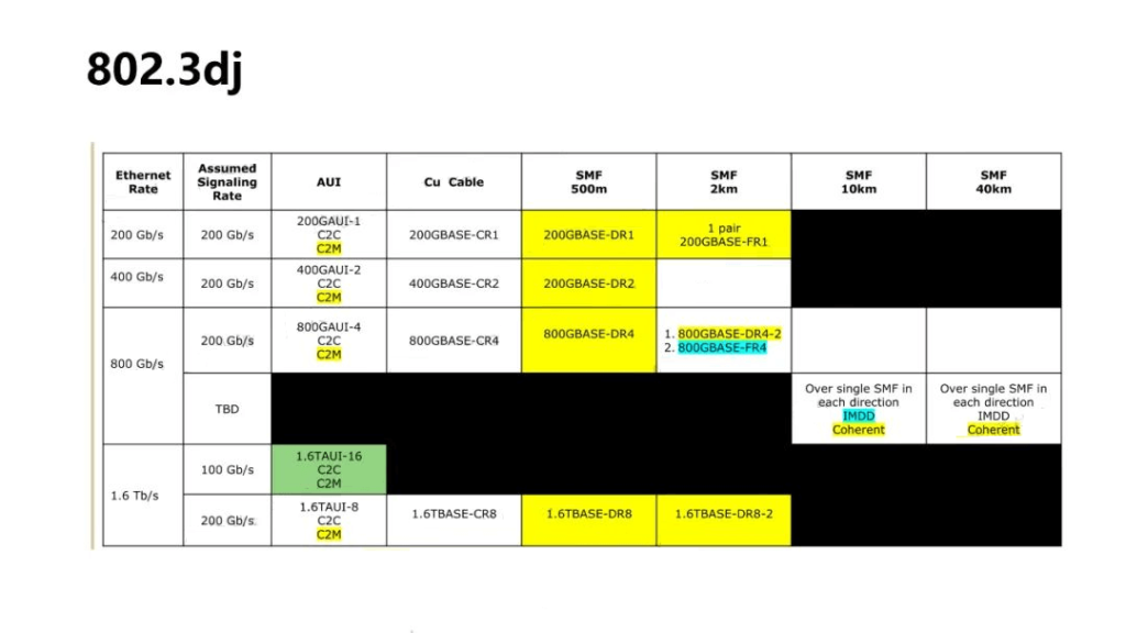
The standards based on 100G/channel for 400G and 800G are currently being discussed in 802.3df, and are expected to be released by the end of 2024.
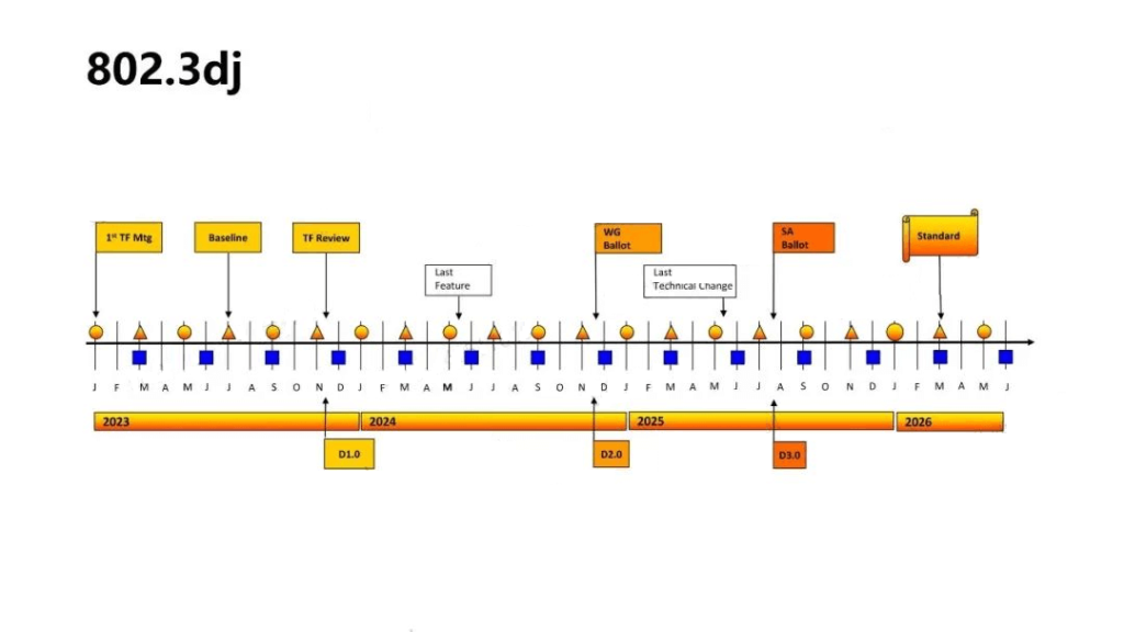
The standards for 400G, 800G, and 1.6T based on 200G/channel are anticipated to be released in 2026.
Although the standards are not yet finalized, the underlying technologies can be traced. For example, the 800G multimode application in 802.3df and the 400G application in the recently released 802.3db both use 100G PAM4 VCSEL, with 802.3df using 8 channels and 802.3db using 4 channels, sharing common ground in chip design and packaging.
Similarly, the 100G EML used in the 2021-released 802.3cu standard can be scaled up to support the 800G 802.3df standard currently under discussion.
Regarding 802.3dj, the key technology of 200G EML, which was first mentioned, can be explored through ongoing experiments and trials, as there are numerous examples of 200G EML chip design and packaging cases.
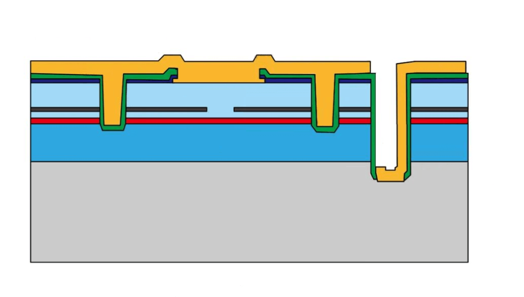
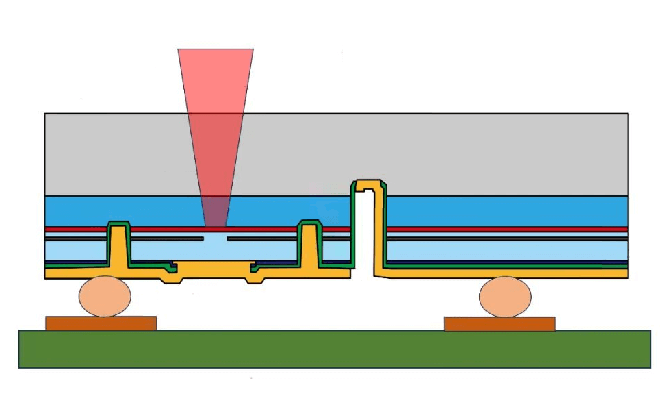
The impact of packaging on bandwidth is limited by the LC resonance frequency, where the parasitic inductance L is mainly caused by the bond wires. Adopting a flip-chip packaging approach can reduce the LC and improve the overall device bandwidth.
Both EML and VCSEL now have flip-chip packaging options. For EML, the light is emitted from the side, so the optical path in the flip-chip substrate is not a concern. For VCSELs, which are top-emitting, the flip-chip approach needs to consider the impact on both the electrical and optical paths.
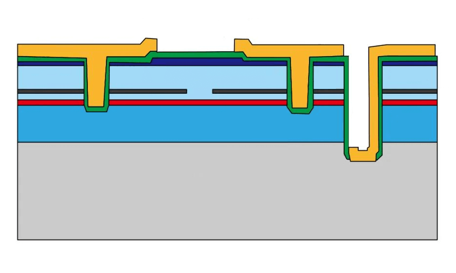
If the VCSEL is top-emitting, a glass substrate (COG, Chip-on-Glass) can be used, which serves as both the electrical and optical interface.
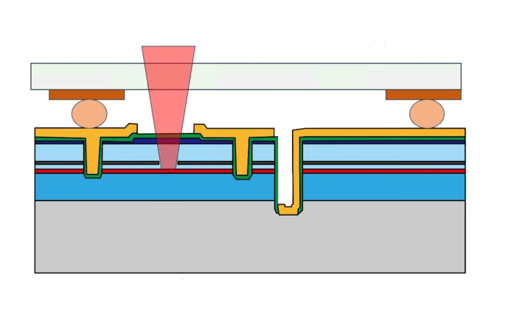
The bandwidth of EML and VCSEL chips is also affected by temperature, as higher temperatures can lead to a reduction in bandwidth. For bottom-emitting VCSELs with flip-chip packaging, in addition to addressing the LC resonance-induced bandwidth changes, the packaging can also help reduce the temperature, further improving the bandwidth.
For bottom-emitting VCSELs, the packaging can use opaque substrates like COC/COB, which is an advantage.
The bottom-emitting VCSEL approach can further reduce the PN junction capacitance, as the P-metal can be used to supplement the resonant cavity, allowing for a reduction in the P-type semiconductor height, and consequently, the PN junction area, within the reliability constraints. In summary, this approach offers advantages in terms of the impact of the PN junction, temperature, and packaging on bandwidth.
The challenge lies in the VCSEL light emission from the substrate, as the traditional GaAs material is not transparent to 850nm. The solutions include either changing the substrate to a material transparent to 850nm or shifting the emission wavelength to 940nm, which is transparent to GaAs.
Related Products:
-
 NVIDIA MMS4X00-NM-FLT Compatible 800G Twin-port OSFP 2x400G Flat Top PAM4 1310nm 500m DOM Dual MTP/MPO-12 SMF Optical Transceiver Module
$1199.00
NVIDIA MMS4X00-NM-FLT Compatible 800G Twin-port OSFP 2x400G Flat Top PAM4 1310nm 500m DOM Dual MTP/MPO-12 SMF Optical Transceiver Module
$1199.00
-
NVIDIA MMA4Z00-NS-FLT Compatible 800Gb/s Twin-port OSFP 2x400G SR8 PAM4 850nm 100m DOM Dual MPO-12 MMF Optical Transceiver Module
$650.00
-
NVIDIA MMS4X00-NM Compatible 800Gb/s Twin-port OSFP 2x400G PAM4 1310nm 500m DOM Dual MTP/MPO-12 SMF Optical Transceiver Module
$900.00
-
NVIDIA MMA4Z00-NS Compatible 800Gb/s Twin-port OSFP 2x400G SR8 PAM4 850nm 100m DOM Dual MPO-12 MMF Optical Transceiver Module
$650.00
-
NVIDIA MMS1Z00-NS400 Compatible 400G NDR QSFP112 DR4 PAM4 1310nm 500m MPO-12 with FEC Optical Transceiver Module
$700.00
-
NVIDIA MMS4X00-NS400 Compatible 400G OSFP DR4 Flat Top PAM4 1310nm MTP/MPO-12 500m SMF FEC Optical Transceiver Module
$700.00
-
NVIDIA MMA1Z00-NS400 Compatible 400G QSFP112 VR4 PAM4 850nm 50m MTP/MPO-12 OM4 FEC Optical Transceiver Module
$550.00
-
NVIDIA MMA4Z00-NS400 Compatible 400G OSFP SR4 Flat Top PAM4 850nm 30m on OM3/50m on OM4 MTP/MPO-12 Multimode FEC Optical Transceiver Module
$550.00