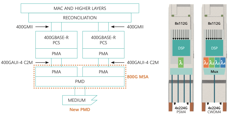
Analysis of technical requirements in 800G FR scenarios
The single-channel 200G-based PAM4 technology, a significant phase of next-generation technology for optical intensity modulation and direct detection interconnect, will be the foundation for 4-channel 800G optical connectivity and an essential building block for future 1.6Tb/s interconnects. As shown in the figure below, the MSA working groups will define the complete PMD and part of the PMA layer specification, including the new low-power, low-latency FEC as a 112G telecom input signal KP4 FEC top package to improve the net coding gain (NCG) of the modem.
One of MSA’s main goals is to develop new broadband, wide-voltage electronic and optical analog components for transmitter and receiver components, including digital-to-analog conversion (DAC) and analog-to-digital conversion (ADC) converters. In order to achieve the low-power goal of pluggable modules, the 200G PAM4 DSP chip will be designed using a lower nm node in the CMOS process, and low-power signal processing algorithms will equalize the channels.
Considering the need for a Thermo Electric Cooler (TEC) in LAN-WDM, which is not required in the 200G per channel solution, the power budget for the 4x200G 800G solution will be based on CWDM4 to analyze the power. Factors related to the power budget include link insertion loss, multipath interference (MPI), differential group delay (DGD), and transmitter and dispersion penalty (TDP).
Based on the model published in the IEEE standard, the MPI and DGD penalties are calculated as shown in the table below. Given that the baud increases to 200G per channel, the dispersion penalty will be greater than the dispersion penalty of 100G per channel. A reasonable recommendation for transmitter dispersion penalty (TDP) is .9 dB. Therefore, considering the margins for receiver aging, coupling losses, and the typical transmitter optical power values, the MSA Working Groups believe that the required receiver sensitivity for 200G PAM4 should be around -5 dBm.

As the baud doubles from 100G to 200G, the OSNR will deteriorate by about 3 dB. Therefore, a more robust FEC error correction code is required to maintain the receiver sensitivity (-5 dBm) and error floor. Therefore, as mentioned above, the optical module needs to consider encapsulating an additional layer of low-power, low-latency FEC on top of the KP4. The error correction threshold of the new FEC can be determined based on the link performance and power budget requirements. The new FEC will be described later.
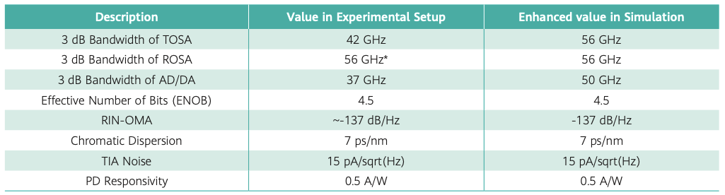
Using simulations and experiments, MSA presents the link performance for a single channel 200G. The following table lists the parameters of the devices used in the link.
The experimental results show that the receiver sensitivity can reach the target value when the new FEC threshold is set to 2E-3 as shown in figure (a) below. However, in this experiment, maximum likelihood sequence estimation (MLSE) is needed to compensate for excessive inter-symbol interference caused by the channel bandwidth limitation.
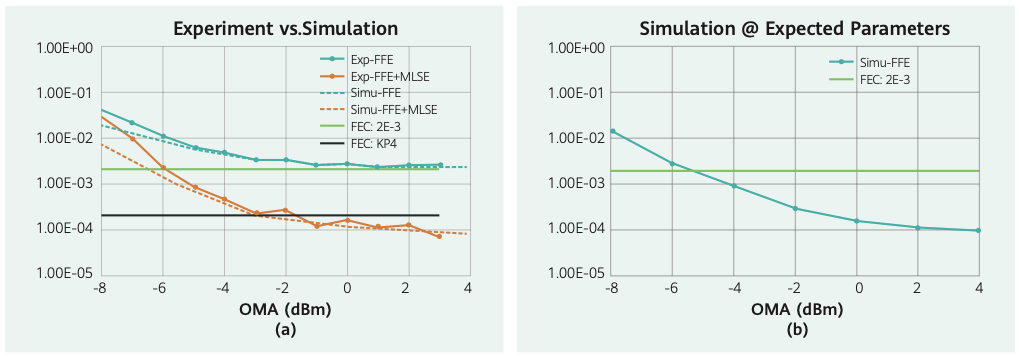
(a) The experimental and simulation results of single-channel 200G match each other; (b) The simulation results of single-channel 200G when the bandwidth of the adopted device is improved: the power budget can be satisfied by using FFE equalization
The dashed line in the above figure (a) shows the results of the simulations using the measured parameters of the devices used in the experiments. Combined with the experimental results, the simulation shows that the system is limited by the bandwidth of components such as AD/DA, drivers, and E/O modulators. The simulation results based on the same system model (bandwidth expansion) are shown in figure (b) above considering the components that are expected to provide higher bandwidth in the coming years and based on the same system model. The results show that with only FFE equalization in the DSP unit, the receiver sensitivity of 2E-3 can be met, as expected from the theory.
Based on the above analysis, it is still recommended to follow TDECQ in the compliance test in the 800G-FR4 scheme. However, the number of FFE taps of the reference receiver used in the TDECQ measurements needs to be considered to increase to a reasonable value, what exactly needs to be further discussed. In addition, it should be noted that if future capabilities for 100Gbaud optical devices are lower than expected, then more complex algorithms (e.g. MLSE) may need to be used in the FR4 scheme, which means that a new compliance scheme for 800G-FR4 will be necessary.
4x200G Packaging Solution Analysis
For the 4x200G optical module, the packaging of its transmitter and receiver needs to be reconsidered to ensure signal integrity in the range of Nyquist frequency points (56GHz). The following figure shows two possible solutions for the emitter. Scheme A is the traditional scheme, where the modulator driver (DRV) and the modulator (such as EML) are next to each other. In scheme B, the DRV chip based on a flip design is packaged together with the DSP unit to optimize the signal integrity on the RF transmission line. Both solutions can be achieved with existing technologies.
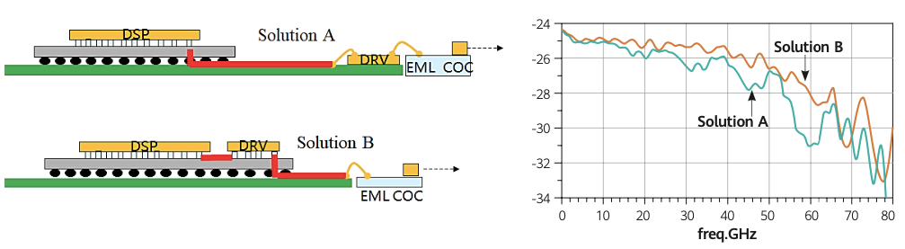
Preliminary simulations show that Scheme B can achieve good results and ensure a bandwidth greater than 56 GHz. The ripple on the S21 curve of Scheme A may be caused by the reflection of the DRV on the input signal, which can be optimized by matching the DRV design to improve the overall performance of Scheme A.
At the receiver, a high-bandwidth photodiode (PD) with less parasitic capacitance and a high-bandwidth trans-impedance amplifier (TIA) is needed to ensure the bandwidth performance of the receiver. There are currently no obstacles to implementing these components through the most advanced semiconductor technology. As far as we know, the industry has put a lot of effort into developing these components and hopefully they will be available in 1 to 2 years. On the other hand, the connection between PD and TIA is also critical. Parasitic effects in the connection can degrade the performance of the module, which also needs to be carefully analyzed and optimized.
Forward Error Correction Coding (FEC) in Single Channel 200G
As mentioned above, a more powerful FEC is required to meet the sensitivity requirement of the 200G PAM receiver, which is a 2E-3 threshold performance for error correction. The figure below illustrates a comparison between the terminated and concatenated schemes.
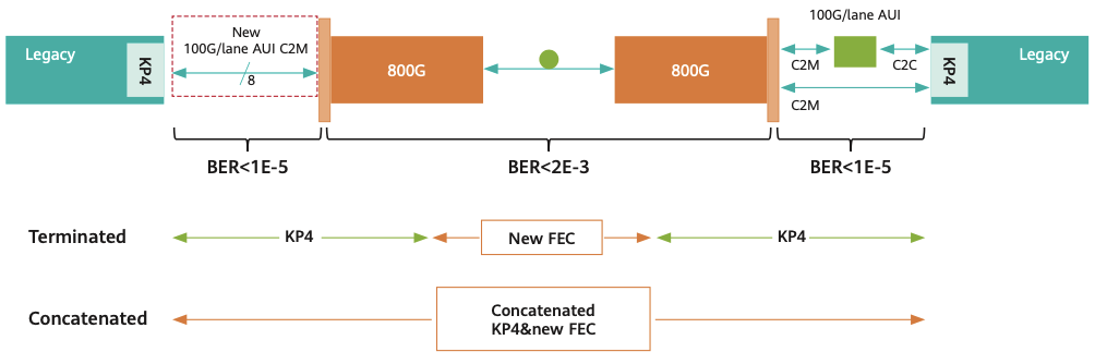
800G FEC: Terminated FEC scheme vs. Concatenated FEC scheme
In the first option, KP4 is terminated and replaced by a new FEC with a larger overhead, which has advantages in terms of NCG and overhead. In the second option, the tandem concatenated scheme keeps KP4 as an external code and merges it with the new internal code. This cascaded tandem approach has more latency and power advantages and is therefore more suitable for 800G-FR4 applications.
Related Products:
-
 NVIDIA MMA4Z00-NS Compatible 800Gb/s Twin-port OSFP 2x400G SR8 PAM4 850nm 100m DOM Dual MPO-12 MMF Optical Transceiver Module
$650.00
NVIDIA MMA4Z00-NS Compatible 800Gb/s Twin-port OSFP 2x400G SR8 PAM4 850nm 100m DOM Dual MPO-12 MMF Optical Transceiver Module
$650.00
-
OSFP-800G-SR8D OSFP 8x100G SR8 PAM4 850nm 100m DOM Dual MPO-12 MMF Optical Transceiver Module
$650.00
-
OSFP-800G-SR8 OSFP 8x100G SR8 PAM4 850nm MTP/MPO-16 100m OM4 MMF FEC Optical Transceiver Module
$650.00
-
OSFP-800G-FR8L OSFP 800G FR8 PAM4 CWDM8 Duplex LC 2km SMF Optical Transceiver Module
$3000.00
-
OSFP-800G-FR8D OSFP 8x100G FR PAM4 1310nm Dual MPO-12 2km SMF Optical Transceiver Module
$1100.00
-
OSFP-800G-FR8 OSFP 8x100G FR PAM4 1310nm MPO-16 2km SMF Optical Transceiver Module
$1200.00
-
OSFP-800G-DR8 OSFP 8x100G DR PAM4 1310nm MPO-16 500m SMF DDM Optical Transceiver Module
$900.00
-
OSFP-800G-2FR4 OSFP 2x400G FR4 PAM4 CWDM4 2km DOM Dual CS SMF Optical Transceiver Module
$1500.00
-
OSFP-800G-DR8D 800G-DR8 OSFP PAM4 1310nm 500m DOM Dual MTP/MPO-12 SMF Optical Transceiver Module
$850.00
-
OSFP-800G-LR8 OSFP 8x100G LR PAM4 1310nm MPO-16 10km SMF Optical Transceiver Module
$1800.00
-
OSFP-800G-LR8D OSFP 8x100G LR PAM4 1310nm Dual MPO-12 10km SMF Optical Transceiver Module
$1800.00
-
QSFP-DD-800G-SR8 800G SR8 QSFP-DD 850nm 100m OM4 MMF MPO-16 Optical Transceiver Module
$850.00
-
QSFP-DD-800G-DR8D QSFP-DD 8x100G DR PAM4 1310nm 500m DOM Dual MPO-12 SMF Optical Transceiver Module
$1250.00
-
QSFP-DD-800G-2FR4L QSFP-DD 2x400G FR4 PAM4 CWDM4 2km DOM Dual duplex LC SMF Optical Transceiver Module
$1800.00
-
QSFP-DD-800G-FR8L QSFP-DD 800G FR8 PAM4 CWDM8 2km DOM Duplex LC SMF Optical Transceiver Module
$3000.00
-
QSFP-DD-800G-2FR4 800G QSFP-DD 2FR4 PAM4 1310nm 2km DOM Dual CS SMF Optical Transceiver Module
$1900.00
-
QSFP-DD-800G-FR8 QSFP-DD 8x100G FR PAM4 1310nm 2km DOM MPO-16 SMF Optical Transceiver Module
$1500.00
-
QSFP-DD-800G-2LR4 QSFP-DD 2x400G LR4 PAM4 CWDM4 10km Dual CS SMF FEC Optical Transceiver Module
$2100.00