According to TrendForce data, AI server shipments were about 130,000 units, accounting for about 1% of global server shipments. Looking ahead to 2023, Microsoft, Meta, Baidu, and ByteDance have successively launched products and services based on generative AI and actively increased orders. It is estimated that the annual growth rate of AI server shipments in 2023 will reach 15.4%, and with the future demand of ChatGPT for AI servers, it is expected that AI servers will grow at a compound annual rate of 12.2% from 2023 to 2027.
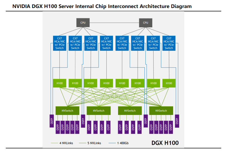
DGX H100 was launched in 2022 and is the latest iteration of NVIDIA’s DGX system, as well as the basis of NVIDIA DGX SuperPOD. DXG servers are equipped with 8 H100 GPUs, and 640 billion transistors, and offer 6 times higher AI performance than the previous generation at the new FP8 precision, providing 900GB/s of bandwidth.
Source: NVIDIA
Inside the DGX H100 server, the blue blocks are IP network cards, which can act as network cards and also play the role of PCIe Switch expansion, becoming the bridge between the CPU and GPU (H100). It uses the PCle 5.0 standard internally. In addition, CX7 is made into 2 cards in the form of network card chips to plug into the server, and each card consists of 4 CX7 chips and outputs 2 800G OSFP optical module ports.
The interconnection between GPUs (H100) is mainly achieved by NV Switch chips. Each GPU in a DGXH100 extends 18 NVLinks outward, with a bidirectional bandwidth of 50 GB/s per link, totaling 18*50GB/s=900GB/s bidirectional bandwidth, which is split to 4 onboard NV Switches, so each NV Switch corresponds to 4-5 OSFP optical modules (a total of 18). Each OSFP optical module uses 8 optical channels, with a transmission rate of 100Gbps per channel, so the total rate reaches 800Gbps, enabling high-speed data transmission.
Interconnection of components such as CPU, GPU: PCIE Switch, Retimer chip
PCIe Switch, also known as PCIe switch or PCIe hub, is mainly used to interconnect PCIe devices, and the communication protocol of the PCIe Switch chip and its device is PCIe. Since PCIe link communication is a kind of end-to-end data transmission, Switch needs to provide expansion or aggregation capabilities, to allow more devices to connect to a PCle port, to solve the problem of insufficient PCIe channel number. Currently, PCIe Switch has not only been widely used in traditional storage systems but also gradually popularized in some server platforms, to improve the speed of data transmission.
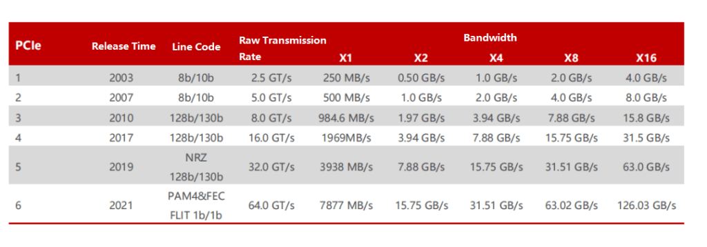
PCIe bus technology upgrade, PCIe Switch speed increase per generation. PCIe bus is a high-speed serial replacement for PCI bus. In 2001, Intel announced the third-generation I/O technology to replace the PCI bus, called “3GIO”. In 2002, this technology was officially renamed “PCI Express” after being reviewed by the PCI Special Interest Group (PCI-SIG), marking the birth of PCIe. In 2003, PCIe 1.0 was officially released, supporting a transmission rate of 250MB/s per channel and a total transmission rate of 2.5 GT/s. In 2007, PCI-SIG announced the launch of PCI Express Base 2.0 specification. Based on PCIe 1.0, the total transmission rate was doubled to 5 GT/s, and the transmission rate per channel increased from 250 MB/s to 500 MB/s. In 2022, PCI-SIG officially released the PCIe 6.0 specification, increasing the total bandwidth to 64 GT/s.
Source: Wikipedia
As PCIe is increasingly applied in servers, the market demand for PCIe Switch is also driven up. According to the statistics and forecast of QYResearch, the global PCIe chip market sales reached 790 million US dollars in 2021, and it is expected to reach 1.8 billion US dollars in 2028, with a compound annual growth rate (CAGR) of 11.9%.
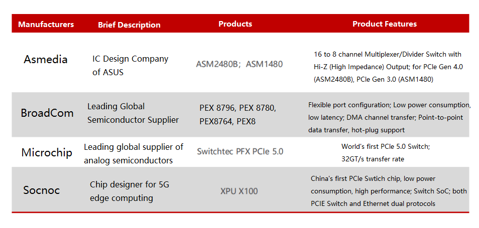
Source: Asmedia, BroadCom, and Microchip
China is the largest market for PCIe Switch. As the demand for massive data storage and transmission in servers increases, a large number of high-speed interconnect solutions are needed to achieve massive data transmission in the fields of big data, cloud computing, artificial intelligence, etc. As a high-speed interconnect solution, PCIe Switch has a great demand in the Chinese market.
In AI servers, at least one Retimer chip is required to ensure the signal quality when the GPU and CPU are connected. Specifically, many AI servers will configure multiple Retimer chips, such as Astera Labs, which configures four Retimer chips in AI accelerator.
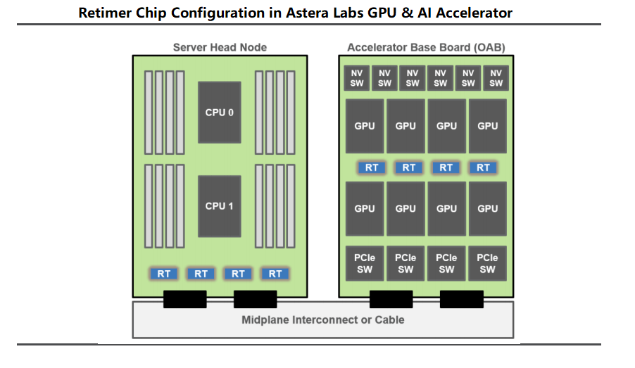
Source: Astera Labs
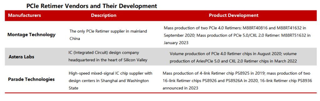
PCIe Retimer is a blue ocean market with three leading manufacturers and many potential competitors. Currently, Parade Technologies, Astera Labs, and Montage Technology are the three major vendors in the PCIe Retimer blue ocean market, occupying the dominant position. Among them, Montage Technology has deployed PCIe earlier and is the only mainland China supplier that can mass-produce PCIe 4.0 Retimer, and its PCIe 5.0 Retimer development is progressing smoothly.
Source: Montage Technology, Astera Labs and Parade Technologies
In addition, chip manufacturers including Renesas, TI, Microchip Technology, and others are also actively involved in the product development of PCIe Retimer. According to the official website information, Renesas can provide two PCIe 3.0 Retimer products, namely 89HT0816AP and 89HT0832P; TI can provide a 16Gbps 8-channel PCIe 4.0 Retimer – DS160PT801; similarly, Microchip Technology released the XpressConnect series of Retimer chips in November 2020, which can support PCIe 5.0’s 32GT/s rate.
GPU-GPU connection: NVLink, NVSwitch
Global chip manufacturers are paying attention to the related technologies of high-speed interfaces. In addition to NVIDIA’s NVLink, AMD’s Infinity Fabric and Intel’s CXL (Compute Express Link) also provide solutions for high-speed interconnection within servers.
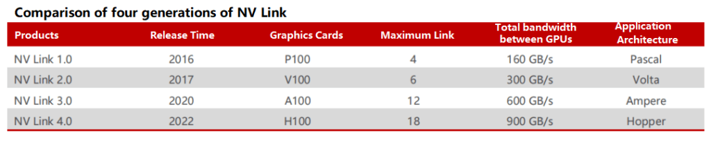
The continuously updated NVlink has sparked a revolution in high-speed interconnection technology. NVLink is a high-speed interconnection technology developed by NVIDIA, which aims to accelerate the data transfer speed between CPU and GPU, GPU and GPU, and improve system performance. From 2016 to 2022, NVLink has iterated to the fourth generation. In 2016, NVIDIA released the new high-speed interface chip – NVLink, carried by the Pascal GP100 GPU. This is the first generation of NVLink. NVLink uses High-Speed Signaling interconnect (NVHS) technology, which is mainly used for signal transmission between GPU and GPU, GPU and CPU. The GPUs transmit differential impedance electrical signals in NRZ (Non-Return-to-Zero) encoding form. The first-generation NVLink single link can achieve 40 GB/s of bidirectional bandwidth, and a single chip can support four links, that is, 160 GB/s of total bidirectional bandwidth.
Source: NVIDIA
NVLink technology has undergone several iterations and updates, sparking a wave of innovation in high-speed interconnection technology. In 2017, the second generation of NVLink based on the Volta architecture was released, which can achieve 50 GB/s of bidirectional bandwidth per link, and support six links per chip, that is, 300 GB/s of total bidirectional bandwidth. In 2020, the third generation of NVLink based on the Ampere architecture was released, which can achieve 50 GB/s of bidirectional bandwidth per link, and support 12 links per chip, that is, 600 GB/s of total bidirectional bandwidth. In 2022, the fourth generation of NVLink based on the Hopper architecture was released, which changed the transmission signal to PAM4 modulated electrical signal, and can achieve 50 GB/s of bidirectional bandwidth per link, and support 18 links per chip, that is, 900 GB/s of total bidirectional bandwidth.
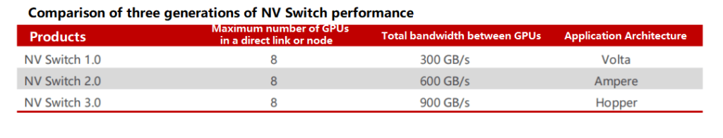
In 2018, NVDIA released the first generation of NVSwitch, which provided a solution for improving the bandwidth, reducing the latency, and enabling communication between multiple GPUs within the server. The first generation of NVSwitch was manufactured using TSMC’s 12nm FinFET process and had 18 NVLink 2.0 interfaces. A server can support 16 V100 GPUs through 12 NVSwitches, achieving the highest interconnection speed with NVLink.
Source: NVIDIA
Currently, NVSwitch has iterated to the third generation. The third generation of NVSwitch is built using TSMC’s 4N process, and each NVSwitch chip has 64 NVLink 4.0 ports. The communication speed between GPUs can reach 900GB/s, and these GPUs connected by NVLink Switch can be used as a single high-performance accelerator with deep learning capabilities.
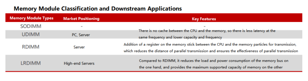
High-speed interconnection between CPU and DRAM drives the demand for memory interface chips.
The main types of server memory modules are RDIMM and LRDIMM, which have higher requirements for stability, error correction, and low power consumption than other types of memory modules. The memory interface chip is the core logic device of the server memory module and is the necessary path for the server CPU to access the memory data. Its main function is to improve the speed and stability of memory data access and meet the growing high-performance and large-capacity needs of the server CPU for memory modules.
Source: CSDN
The speed of memory interface chips continues to increase from DDR4 to DDR5. Since 2016, DDR4 has become the mainstream technology in the memory market. To achieve higher transmission speed and support larger memory capacity, the JEDEC organization further updated and improved the technical specifications of DDR4 memory interface chips. In the DDR4 generation, from Gen1.0, Gen1.5, and Gen2.0 to Gen2plus, the highest transmission speed supported by each sub-generation of memory interface chips has been continuously increasing, and the last sub-generation product of DDR4, Gen2plus, supports a maximum transmission of 3200MT/s. As the JEDEC organization continues to improve the specification definition of DDR5 memory interface products, DDR5 memory technology is gradually replacing DDR4 memory technology.
Currently, DDR5 memory interface chips have planned three sub-generations, with support rates of 4800MT/s, 5600MT/s, and 6400MT/s respectively. The industry expects that there may be 1-2 more sub-generations in the future.
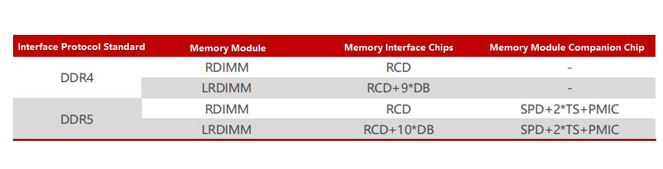
Memory interface chips are divided into two types according to their functions, namely register buffer (RCD) and data buffer (DB). RCD is used to buffer the address, command, and control signals from the memory controller, and DB is used to buffer the data signals from the memory controller or memory granules.
Source: Montage Technology
Upgrading DDR5 memory modules brings new opportunities for memory interface chips and module-supporting chips. In 2016, the global memory interface chip market size was about 280 million US dollars, and it reached about 570 million US dollars in 2018, with a three-year annualized growth rate of 40%. The upgrade of DDR5 will bring the market size of memory interface chips to a new level. Compared with DDR4, due to the higher support rate and more complex design of DDR5, the starting price of the first sub-generation of DDR5 memory interface chips is higher than that of DDR4 memory interface chips. At the same time, as the penetration rate of DDR5 memory in servers and PCs gradually increases, the market size of DDR5-related memory interface chips is expected to achieve rapid growth.
The memory interface chip industry has high barriers, and a three-legged pattern has been formed. Memory interface chips are a technology-intensive industry, and they can only be used on a large scale after being strictly verified by CPU, memory, and OEM manufacturers in all aspects, and new players are difficult to enter. With the increasing technical difficulty, the number of memory interface chip players has decreased from more than 10 in the DDR2 generation to only 3 in the DDR4 generation. The industry has cleared out, and a three-legged pattern has been formed. In the DDR5 generation, there are only three suppliers in the world that can provide mass-produced products of the first sub-generation of DDR5, namely Montage Technology, Renesas Electronics (IDT), and Rambus.
Related Products:
-
 NVIDIA MMA4Z00-NS400 Compatible 400G OSFP SR4 Flat Top PAM4 850nm 30m on OM3/50m on OM4 MTP/MPO-12 Multimode FEC Optical Transceiver Module
$550.00
NVIDIA MMA4Z00-NS400 Compatible 400G OSFP SR4 Flat Top PAM4 850nm 30m on OM3/50m on OM4 MTP/MPO-12 Multimode FEC Optical Transceiver Module
$550.00
-
NVIDIA MMA4Z00-NS-FLT Compatible 800Gb/s Twin-port OSFP 2x400G SR8 PAM4 850nm 100m DOM Dual MPO-12 MMF Optical Transceiver Module
$650.00
-
NVIDIA MMA4Z00-NS Compatible 800Gb/s Twin-port OSFP 2x400G SR8 PAM4 850nm 100m DOM Dual MPO-12 MMF Optical Transceiver Module
$650.00
-
NVIDIA MMS4X00-NM Compatible 800Gb/s Twin-port OSFP 2x400G PAM4 1310nm 500m DOM Dual MTP/MPO-12 SMF Optical Transceiver Module
$900.00
-
NVIDIA MMS4X00-NM-FLT Compatible 800G Twin-port OSFP 2x400G Flat Top PAM4 1310nm 500m DOM Dual MTP/MPO-12 SMF Optical Transceiver Module
$1199.00
-
NVIDIA MMS4X00-NS400 Compatible 400G OSFP DR4 Flat Top PAM4 1310nm MTP/MPO-12 500m SMF FEC Optical Transceiver Module
$700.00
-
NVIDIA(Mellanox) MMA1T00-HS Compatible 200G Infiniband HDR QSFP56 SR4 850nm 100m MPO-12 APC OM3/OM4 FEC PAM4 Optical Transceiver Module
$139.00
-
NVIDIA MFP7E10-N010 Compatible 10m (33ft) 8 Fibers Low Insertion Loss Female to Female MPO Trunk Cable Polarity B APC to APC LSZH Multimode OM3 50/125
$47.00
-
NVIDIA MCP7Y00-N003-FLT Compatible 3m (10ft) 800G Twin-port OSFP to 2x400G Flat Top OSFP InfiniBand NDR Breakout DAC
$260.00
-
NVIDIA MCP7Y70-H002 Compatible 2m (7ft) 400G Twin-port 2x200G OSFP to 4x100G QSFP56 Passive Breakout Direct Attach Copper Cable
$155.00
-
NVIDIA MCA4J80-N003-FTF Compatible 3m (10ft) 800G Twin-port 2x400G OSFP to 2x400G OSFP InfiniBand NDR Active Copper Cable, Flat top on one end and Finned top on other
$600.00
-
NVIDIA MCP7Y10-N002 Compatible 2m (7ft) 800G InfiniBand NDR Twin-port OSFP to 2x400G QSFP112 Breakout DAC
$190.00