Optical module (Figure 1) is an important component in the optical communication system, the main function is to realize the photovoltaic conversion and the monitoring and management of communication signals and other functions. In today’s optical fiber network, the application scenarios of optical transceivers are increasing. For example, when we make a phone call with a mobile phone, there is radio communication between the mobile phone signal and the base station. The optical module is needed when the base station is connected to the server through an optical fiber link. Optical transceivers are also needed for optical fiber broadband networks to the home and for the interconnection of a large number of switches in data centers.
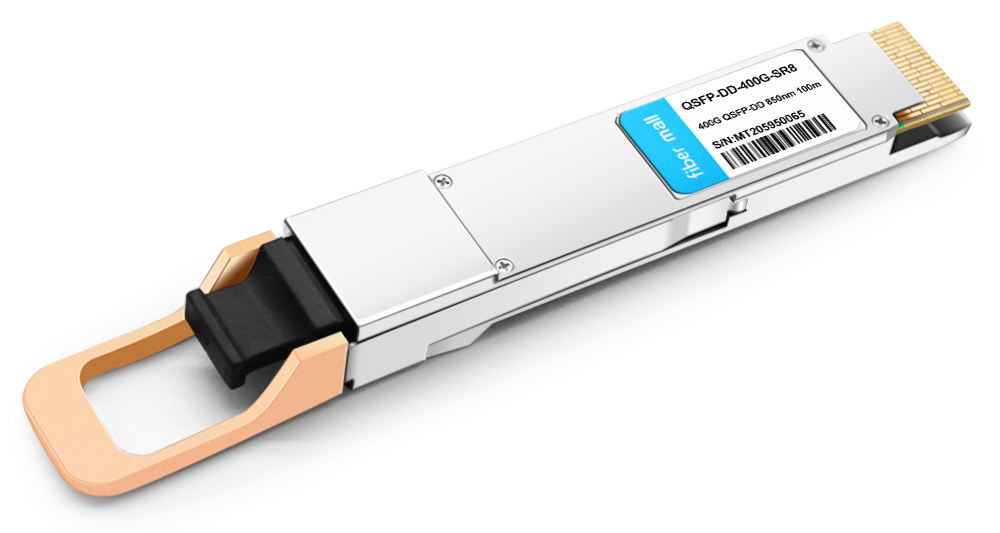
Figure 1. Optical Transceiver (400G QSFP-DD SR8)
Market demand for optical modules
According to Lightcounting, the global optical module market is expected to reach $8.132 billion in 2022 and is expected to grow at a compound annual growth rate of 13.7% from 2021 to 2026. Among them, the proportion of data center application optical module has exceeded that of telecom market optical module, and it is expected to take up more than 55% in 2022. Figure 2 shows the global market and capital expenditure analysis for optical modules.
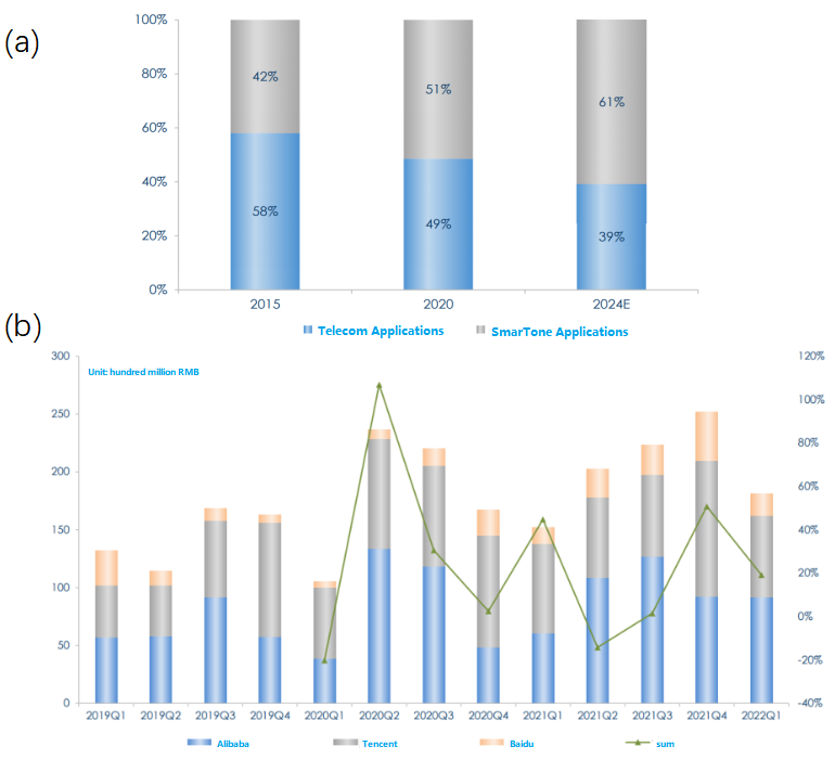
Figure 2. Global market and capital expenditure of optical modules. (a) Application areas of the global optical module market. (b) Capital expenditure of Chinese cloud vendors.
Overall capital expenditures for data centers continue to expand rapidly. According to Cignal AI’s long-term forecast, computing and storage cloud infrastructure spending will grow at a compound annual growth rate (CAGR) of 12.6 percent from 2021 to 2026. Changes in online lifestyles of work in the post-epidemic era, public cloud (public cloud refers to cloud services provided to users by third-party providers via the public Internet, where users can access the cloud and enjoy various services including and not limited to computing, storage, networking, etc.) With the global expansion of giants and the rapid landing development of AI in various industries, data center investment maintains strong momentum, making the boom of data center optical module market continue to rise.
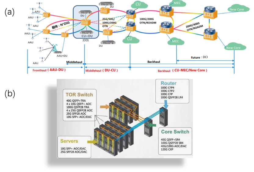
Figure 3. Application scenario of optical module in telecommunication market and data center. (a) 5G telecommunications network architecture; (b) Data centre ridge server architecture
COB Packaging Technology
According to the different application scenarios and requirements, optical modules can be broadly divided into carrier-grade and data-center optical modules. The carrier-grade optical transceiver is applied to harsh environmental conditions and difficult to replace and maintain. The data center optical transceiver is applied to relatively mild environment and convenient to maintain. For example, carrier-grade optical modules used in the outdoor base stations may face a high-temperature working environment of 80℃ when the sunshine is strong, while the ambient temperature in the winter nights in the north may be as low as -40 ℃. At the same time, in order to guarantee signal coverage, these base stations may be located in mountainous and inaccessible places, making it difficult to perform regular maintenance. All these characteristics determine the high requirements for reliability assurance of carrier-grade optical modules.
In the application scenario of a data center, the data center may be in an equipment room with air control, temperature control and humidity control. Resident maintenance personnel can perform maintenance at any time. Therefore, the reliability requirement is relatively low. Considering the application scenario, requirement and cost, different optical module packaging technologies have been developed.
Currently, carrier-grade optical modules mostly use hermetic To-can or BOX packaging technology. Data center optical modules mostly use non-hermetic COB packaging technology, as shown in Figure 4. The full name of COB is chip on board, that is, chip on board packaging. The bare chip is attached to the PCB with conductive or non-conductive adhesive, and then the electrical connection is realized by lead bonding, and the chip and bond lead are wrapped with adhesive. The packaging technology was first widely used in the packaging of LED, and later introduced into the packaging of optical modules.
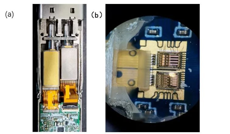
Figure 4. (a) BOX package optical module diagram. (b) COB package optical module diagram
Technical advantages of optical module COB packaging
- Better high-speed signal connection performance
With hermetically sealed carrier-grade optical transceivers, the laser is connected to the PCB through FPC (Flexible Printed Circuit) and high-frequency ceramics before being connected to the laser through gold wire. It is difficult to guarantee impedance continuity at multiple connection points and signal integrity loss is inevitable. In the COB package, the laser can be directly connected with the PCB through the gold wire bonding, which greatly reduces the impedance discontinuities and better guarantees the connection of high-speed signals from the PCB to the LD, thus showing a larger margin of eye diagram template and higher sensitivity performance.
- Ability to reduce size and cost
COB package saves space because it saves high frequency ceramic box, flexible cable and other components. Its advantages are more obvious today as optical modules continue to pursue more miniaturized packages. Take a 400G QSFP-DD optical module with EML laser as an example (Figure 5), it requires a large number of electrical chips such as DML bias, EA bias, EA modulation, DSP, etc. The optical part requires components such as EML, isolator, lens, etc. If the hermetic package is used, the optical components will occupy a large space, greatly compressing the arrangement space of the electrical components and posing a great challenge to the module design. While using COB package, the space saved can give the electrical to improve more redundant design, such as adding more filter capacitors, larger high-frequency signal isolation layout, thus improving the module performance.
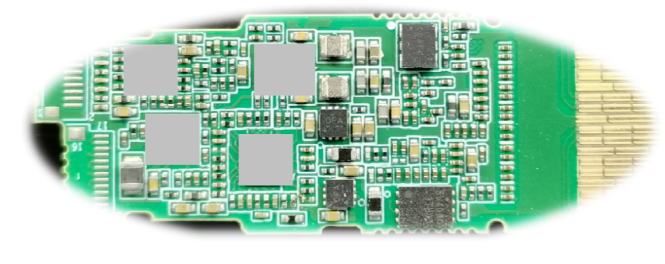
Figure 5. 400G optical module diagram, small size requirements and a large number of components bring challenges to package design
In terms of cost, COB package saves components such as high-frequency ceramic box and flexible cable, and process steps such as nitrogen-filled welding and sealing, BOX leak detection, FPC welding, and separate testing of optical devices, which can reduce material cost and production cost.
Disadvantages of COB packaging for optical modules
- Reduced life of sensitive devices
In COB package, the optical devices and some electrical chips, such as drivers and TIAs, are directly exposed, leading to adverse effects on service life. While in the hermetic package, LDs are sealed in a box filled with nitrogen, which is isolated from the external environment and better protects the stable operation of LDs.
In recent years, module manufacturers have also developed some limited hermetic sealing techniques to prolong the life of LD in COB modules, drawing on both packaging technologies. For example, if the LD is mounted in a semi-open metal box, the PCB can enter the metal box through the openings to connect directly with the LD, while the metal box can be sealed by glue to provide a certain degree of hermeticity.
- Not conducive to defective product rework
In BOX package, optical devices can be completely separated from the PCB and tested separately. Any part of the problem can be replaced and repaired separately.
In the COB module, since the optical device is directly connected to the PCB board, the performance test can only be carried out after the whole production is completed. In case of defects, it is more difficult to check whether the fault is electrical chip or optical chip, and it is more likely to cause scrap when the device is reworked and replaced. There may be an optical chip damage, resulting in the scrapping of the entire module, which to a certain extent increases the scrapping rate of the entire production process. Therefore, the COB packaging process, process stability and yield rate is particularly important.
Key technical steps for COB packaging of optical modules
The main process steps of COB package optical modules include die bonding, wire bonding, optical coupling, and testing (Figure 6).
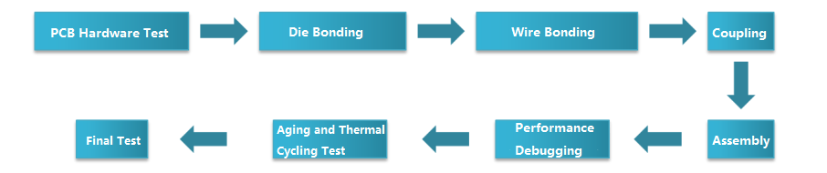
Figure 6. COB Packaging process of optical module
Die bonding is to glue various types of chips to the PCB, such as clock recovery chips, laser driver chips, trans-impedance amplifier chips, laser chips, and detector chips in data center optical module, and commonly used conductive adhesive directly attached on PCB. In the mounting, we should pay attention to whether the position precision meets the requirements, whether the chip bonding is firm, etc. For the laser, driver power consumption is large, high heat generation chip, we also need to pay attention to the contact heat dissipation performance after mounting.
Wire bonding refers to the electrical connection between the pins of the chip and the pads on the PCB through wires, usually using gold wire bonding technology (Figure 7). This step should pay attention to whether the wire connection is in good contact and whether there is virtual connection. It is usually checked by wire pull. In high-speed optical modules, the lines are often complex and require a lot of cross-hitting, which requires attention to whether there are problems such as collapsed lead laps. For the connection of high-speed signal pins, attention should be paid to the length and number of leads, which are generally used to reduce the lead length and increase the number of leads to enhance the signal integrity.
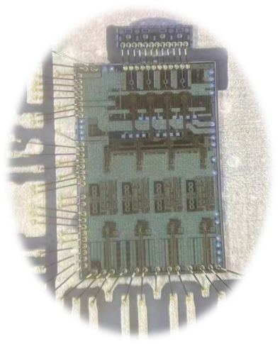
Figure 7. Wire bonding
Coupling (Figure 8) is the longest working time and most likely defective step in optical module packaging. For multi-mode optical modules, surface-emitting laser (VCSEL) is commonly used, which is coupled into the multi-mode fiber through the mirror.
The light path is simple, the tolerance is large, and the process is relatively simple. Single-mode fiber is much more complicated because the core diameter of single-mode fiber is smaller than that of multi-mode fiber, only 9μm, which requires a lens for focusing coupling. In the module that needs multiplexed coupling, such as LR4, it is necessary to add and split wave elements, which further increases the complexity of the optical path. An important auxiliary material for coupling is UV-curable adhesive, which is mainly used for bonding coupling lenses. It is characterized by fast curing of the glue after ultraviolet irradiation, low shrinkage rate, and suitable for collimating coupling lenses with high requirements for bonding and fixing accuracy.
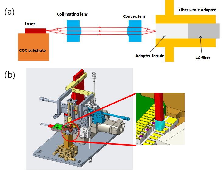
Figure 8. coupling in COB packaging
Testing is the final step in the production of optical modules, which is mainly divided into performance testing and reliability testing. Common performance test items include eye diagram margin, extinction ratio, transmit power, receive sensitivity, etc. Reliability test items usually include high and low temperature charged aging test, high and low temperature cyclic shock test, vibration test, multiple plugging test, etc.
Trends in Data Center Optical Module Packaging Technology
Overall, the demand trend for data center optical modules is more miniaturized package, higher transmission rate and lower cost. At present, 100G QSFP28 optical modules have been widely used in data centers, 400G QSFP-DD optical modules have been commercially available in large-scale data centers, and 800G QSFP-DD800 optical modules are in the early stage of commercialization. In the face of the demand for higher speed, traditional optical module packaging is facing more and more difficulties, including the increase in package complexity, lower yield leading to increased costs, and limited device bandwidth. In this context, the commercialization of new technologies such as silicon optical modules and co-packaged optics (CPO) is more expected.
The application of silicon photonics in optical modules aims to simplify the process and reduce costs by integrating originally discrete optical components, such as modulators, detectors, MUX/DeMUX, lenses, prisms, etc., through a highly integrated silicon photonics chip. At present, silicon photonics chips have been able to integrate detectors, high-speed modulators, waveguides, WDM, and other devices on the same silicon-based substrate, and are expected to be able to integrate more electrical chips such as CDR and TIA in the future, greatly enhancing the integration of optical modules.
400G QSFP-DD silicon photonics modules are already entering the market in volume in 2022. Market research firm Yole forecasts that silicon photonics modules will reach $3.67 billion by 2025, making them a significant part of the optical module market. Figure 9 illustrates the various types of silicon photonics devices.
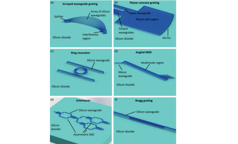
Figure 9. silicon photonics devices
Co-packaged optics technology has been gaining more and more attention in recent years, which has great advantages over traditional pluggable optical modules in terms of electrical connection loss. By packaging the photoelectric chip and the switching chip together, CPO technology can greatly shorten the length of the high-frequency wire, thus solving the problem of serious attenuation of the electrical signal at higher speeds. CPO technology also has great advantages over the pluggable form in terms of bandwidth, size, weight, and power consumption.
However, CPO technology still has some problems to be further solved, including the high-density photoelectric PCB board process, high-precision photoelectric chip packaging process and heat dissipation design, and the reliability of highly integrated photoelectric chips. CIR forecasts that the CPO market is expected to reach $5.4 billion in 2027. Figure 10 shows the evolution of on-board connection technology.
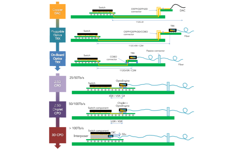
Figure 10. Evolution of on-board connection technology
Related Products:
-
 QSFP28-100G-SR4 100G QSFP28 SR4 850nm 100m MTP/MPO MMF DDM Transceiver Module
$40.00
QSFP28-100G-SR4 100G QSFP28 SR4 850nm 100m MTP/MPO MMF DDM Transceiver Module
$40.00
-
QSFP28-100G-IR4 100G QSFP28 IR4 1310nm (CWDM4) 2km LC SMF DDM Transceiver Module
$110.00
-
QSFP28-100G-SRBD Dual Rate 40G/100G QSFP28 BIDI 850nm & 900nm 100m LC MMF DDM Optical Transceiver
$449.00
-
QSFP28-100G-LR4 100G QSFP28 LR4 1310nm (LAN WDM) 10km LC SMF DDM Transceiver Module
$285.00
-
NVIDIA(Mellanox) MMA1T00-HS Compatible 200G Infiniband HDR QSFP56 SR4 850nm 100m MPO-12 APC OM3/OM4 FEC PAM4 Optical Transceiver Module
$139.00
-
NVIDIA(Mellanox) MMS1W50-HM Compatible 200G InfiniBand HDR QSFP56 FR4 PAM4 CWDM4 2km LC SMF FEC Optical Transceiver Module
$650.00
-
QSFP-DD-400G-SR8 400G QSFP-DD SR8 PAM4 850nm 100m MTP/MPO OM3 FEC Optical Transceiver Module
$149.00
-
QSFP-DD-400G-DR4 400G QSFP-DD DR4 PAM4 1310nm 500m MTP/MPO SMF FEC Optical Transceiver Module
$400.00
-
QSFP-DD-400G-LR4 400G QSFP-DD LR4 PAM4 CWDM4 10km LC SMF FEC Optical Transceiver Module
$600.00
-
QSFP-DD-400G-ER4 400G QSFP-DD ER4 PAM4 LWDM4 40km LC SMF without FEC Optical Transceiver Module
$3500.00