800G Optical Transceiver: SR8 vs DR vs FR vs LR vs FR4 vs LR4 vs FR8
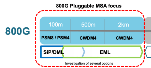
The sponsors of the 800G pluggable MSA are mainly Chinese and Japanese companies, including mainly China Telecom Technology Laboratory, H3C, Huawei, Sumitomo, Tencent, and Yamazaki. The goal is to define pluggable low-cost optical modules for data center applications with short-range 800G transmission, including 8X100G and 4X200G specifications, with transmission distances including 100m, 500m, and 2km, as shown in the figure below.
There are currently some views in the industry that 800G transmission needs will emerge in 2021, and the market will begin to mature by 2023. Correspondingly, there is a QSFP-DD800 MSA optical module working group led by US communications giant Broadcom and Cisco to promote the standardization of 800G optical modules and related connectors in QSFP-DD format.
Figure 1. The research scope of 800G MSA
The general content of this article:
1. New applications (cloud computing, AI applications) have brought about the demand for higher interconnection bandwidth, and the industry needs faster optical modules, such as 800G;
2. Data center architecture and bandwidth requirements of switches in different locations;
3. SR interconnection scenario requirements, 8x100G solution technical analysis;
4. Need analysis of FR to interconnect scenario, the feasibility of 4x200G technology, key technology;
5. Potential technical solutions for DR Scenarios;
6. Summary and outlook.
Figure 2. 800G MSA main driving companies
1. Background - 800G market is coming
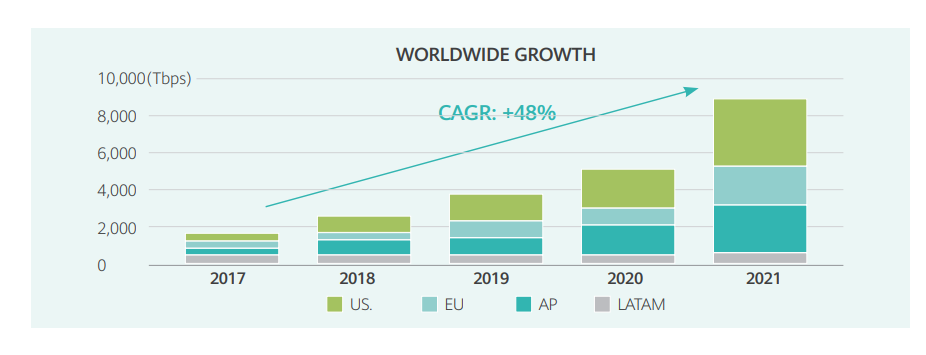
According to Fiber Mall research, new applications such as AR/VR, AI, and 5G will generate increasing amounts of traffic and grow exponentially. This will lead to the need for more bandwidth and more connections, as shown in the figure. Global interconnect bandwidth capacity will continue to grow rapidly over the next four years, with a compound growth rate of 48%.
Figure 3. Global Interconnection Index
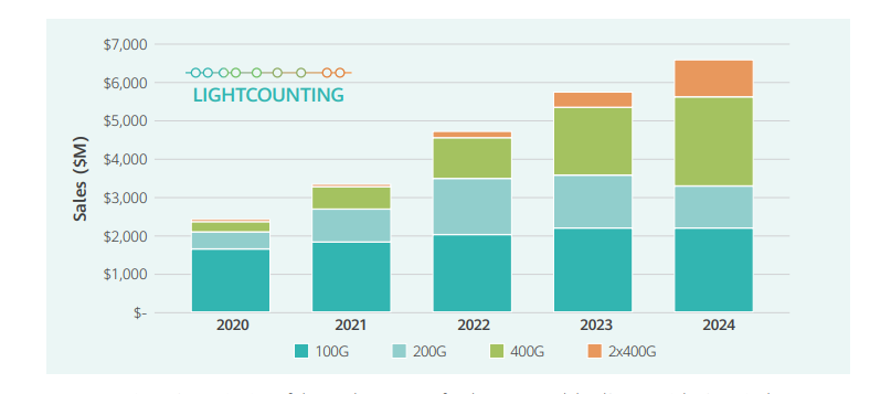
The corresponding market to demand also reflects this trend. As shown in Figure 4, light counting predicts that 400G optical modules in the data center market will grow rapidly in the next five years, and a 2x400G or 800G market will appear around 2022. According to Vladimir, Ph.D., CEO of Lightcounting market Research, cloud data center operators will be deploying 800G QSFP-DD and 800G OSFP optical modules in 2023 to 2024 to cope with growing network traffic. Most of these optical modules will be pluggable, and it is possible to see modules co-packaged.
Figure 4. Annual sales forecast of the Data center optical module market
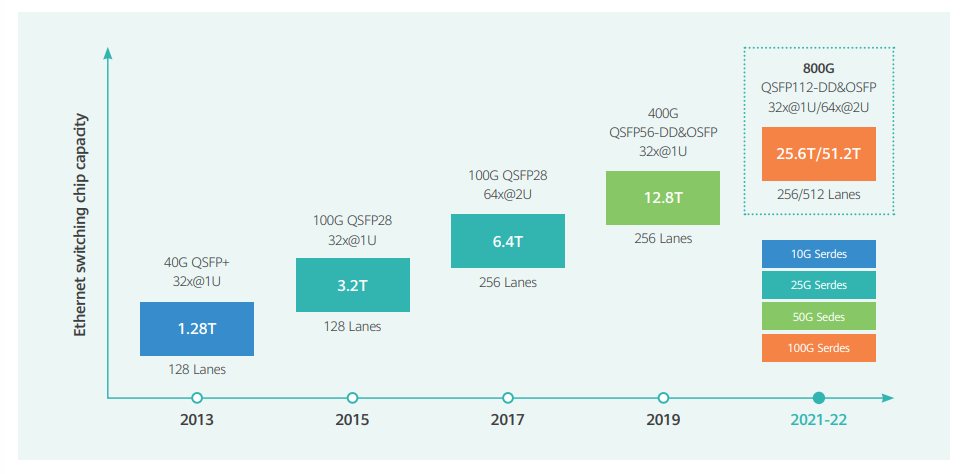
As Moore's Law of doubling capacity in two years has not yet expired in the switching ASIC chips, the architecture of cloud data centers will be challenged by capacity expansion. The current commercially deployed Ethernet switches have a capacity of 12.8Tb/s, though they will face replacement by 25.6Tb/s in 1 year. The capacity evolution path for switches is shown in Figure 5, which will put tremendous pressure on high-density optical interconnects. This is because not all optoelectronic devices can double their integration density every two years as CMOS processes do. This is determined by the differences in devices, design, and manufacturing methods.
Figure 5. Data center switching chip capacity evolution law
In the past few years, 100G short-range optical modules based on NRZ direct probing have made a big splash, carrying most of the fast-growing traffic for cloud services. Since the IEEE initiated research on 400GE-related standards in March 2011, it has ushered in the deployment of 400G QSFP-DD optical modules at scale in 2020 and the demand will be even stronger next year. Figure 4 illustrates this growth trend. It is worth noting that in the early stage of application, 400G QSFP-DD modules are mainly used for transmission in DR4 scenarios with 4x100G rates and distances up to 500m, as well as FR4 scenarios with 2x200G rates and distances up to 2km, the 400GE MAC function is not really used. At the same time, it is also noted that the IEEE may not standardize 800GE optical ports in the short term, at least in the last two years it will not complete 8x100GE or 2x400GE high-density interconnection of 800GE standard. But by then the actual demand for 800G has emerged, so the industry needs to develop specifications to achieve interconnection and interoperability of 800G optical module products from different manufacturers.
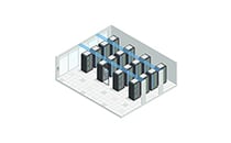
2. Data Center Architecture
In general, the data center architecture and traffic characteristics may differ depending on the application being served. For example, the main traffic in a data center that provides XaaS-type services for external customers is more likely to be north-south server-to-client, in which case the data center size can be more geographically concentrated. In contrast, in a cloud or storage-oriented data center for internal needs, traffic is more likely to flow east-west server-to-server, which typically requires a concentration of mega data center resources. Even though the application scenarios are similar, operators can still choose PSM4 or CWDM4-based optical interconnect solutions based on their own preferences. This leads to a diversity of data center architectures and technologies.
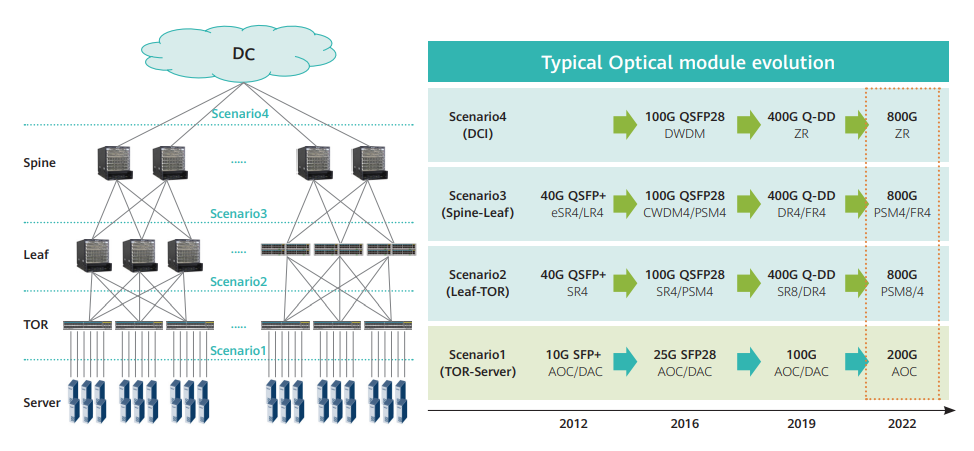
There are at least two common data center architectures. The figure below shows a typical data center architecture (3 tiers) and its switching rate evolution roadmap. However, a typical data center will have more devices than the one in the figure and the architecture will appear larger and more complex. The convergence ratio of about 3:1 is considered among each layer. For example, one Spine switch may be connected to three Leaf switches, and so on. On top of the Spine layer, a coherent optical interconnection solution of type ZR is needed to achieve interconnection with other data centers (DCI scenario). The symbol of the 800G interface rate is that when the rate between sever and TOR switch reaches 200G, the PSM4 4x200G fan out structure between TOR and Leaf as well as the Spine layer has to be adopted.
Figure 6. Common Layer 3 Data Center Architectures and Optical Interconnect Rate Evolution
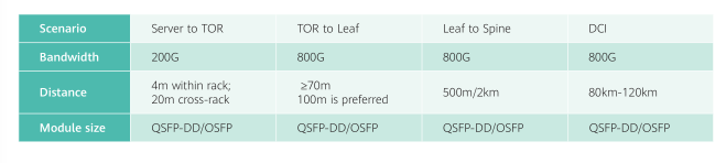
The TOR, Leaf, and Spine switches here actually correspond to the access layer, aggregation layer, and core layer. For a typical data center network (DCN), 800G of network connection bandwidth is required if 200G of server bandwidth is deployed. However, some trade-offs can be made in the capacity of the data center to provide services (bandwidth, transmission distance, and other resources) based on the data center construction budget. As in Table 1, the bandwidth and transmission distance requirements for different tiers in the data center network are given, and the recommended optical module package size requirements are given.
Table 1. Bandwidth and transmission distance requirements for different layers of DCN
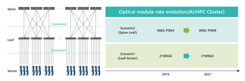
Considering the massive computing demands of the recently emerging AI applications, a two-layer switching architecture is usually adopted in some AI application-oriented supercomputer clusters or AI data centers, as shown in Figure 7. This is because, considering the characteristics of AI computing, there is no need for traffic aggregation between layers. As the traffic of each server is already very large, it directly corresponds to a switch interface and enjoys exclusive bandwidth resources. It can be seen that the traffic characteristics of this AI or supercomputer data center network are different from those of conventional data centers. It is mainly large-particle traffic services that do not need a frequent exchange.
Figure 7. AI/HPC Data Center Network Architecture and Rate Demonstration
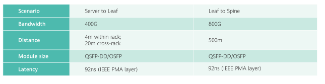
This layer 2 data center network does not require traffic aggregation between layers. If 400G servers are deployed, 800G network interconnection bandwidth is required. Compared with the traditional three-layer switched data center network, this two-layer architecture is more convenient for rapid deployment and has lower latency, which is very suitable for future AI or supercomputer DCN. Table 2 shows the specific technical indicators of this DCN.
Table 2. AI or HPC data center network requirements
However, in some small companies or small cloud data center networks, the transfer rate between Leaf and servers may not require as much bandwidth as 400G, which requires a specific design that considers the relationship between the actual application scenarios faced and the cost.
Let's talk about what you should look for in data center construction. The two most important factors that should be looked at in a data center solution are scalability and cost. When designing a data center, cost control and performance cannot be built to a standard that is too high or too low. If users overbuild, then there will be wasted resources, although these resources can be used to expand more business. But idle resource capacity is expensive, and that capacity can become obsolete technology when it is actually needed to be used. For example, if a user builds a data center with an expected life cycle of 10 years and has built-in additional capacity to accommodate future growth, that capacity may become obsolete in five years. By that time advances in power consumption, performance, and other features can put data center operations and maintenance at a significant disadvantage.
Data centers can also be challenging if they are built to a lower standard, and can even be more expensive. If the user's ability to design rules falls short of the planned requirements, there will be a significant capital expenditure when expanding and upgrading the data center.
It is because of the above possible data center construction over or under the problem, so the rapid expansion of the data center, convenient operation, and cost of these major issues are the priorities of many enterprises.
It is due to the aforementioned possible overbuilding or underbuilding of data centers. Therefore the major issues of rapid data center expansion, ease of operation, and cost are priorities for many enterprises. For the most flexible solution, enterprises often choose the data center hosting model. Data center hosting operators allow users to "pay on demand, scale up incrementally." Users can expand or reduce the rented space as needed, and only pay the associated usage fee. This removes unused or underutilized capacity from the user, removes all the infrastructure-related issues, and maximizes the value of their IT investment.
However, this is not a problem for some Internet giants, who are more concerned about the value of data itself, so they will not hesitate to invest a lot of money to build their own data centers and provide their own cloud services, holding key assets in their own hands. For example, Alibaba, Tencent, Baidu, Facebook, Google, and even some of them have dedicated network infrastructure-related research departments, researching various low-cost and high-speed optical interconnection solutions, even the optical module to develop their own. The goal is to build a better network of data centers, provide faster and more diverse services, and attract more users.
Finally, it's worth explaining why data center networks have become so popular in recent years. It all starts with video. Cisco's latest VNI traffic forecast, shown below, shows that video traffic has become an increasingly important part of the network in recent years, and is expected to account for more than 80% of all Internet traffic by 2022. This will come as no surprise to you, as we are the recipients and producers of video traffic every day. The rise of video service is the change of the bearer network architecture and traffic distribution. With the construction of content distribution networks (CDN) and the sinking of data center networks (DCN), content, such as videos and files, is being cached closer to the user, providing lower latency and faster buffering. Most of the traffic would no longer need to travel over long distances in the backbone network but would end up within the range of short - and medium-distance metropolitan area networks or data center networks. As early as 2017, there was a report that short - and medium-distance MAN traffic had surpassed long-distance backbone traffic. Data center, especially cloud Data Center Interconnection (DCI), is the most typical application of metro networks. Therefore, it is not surprising that the topic of it is hot in recent years.
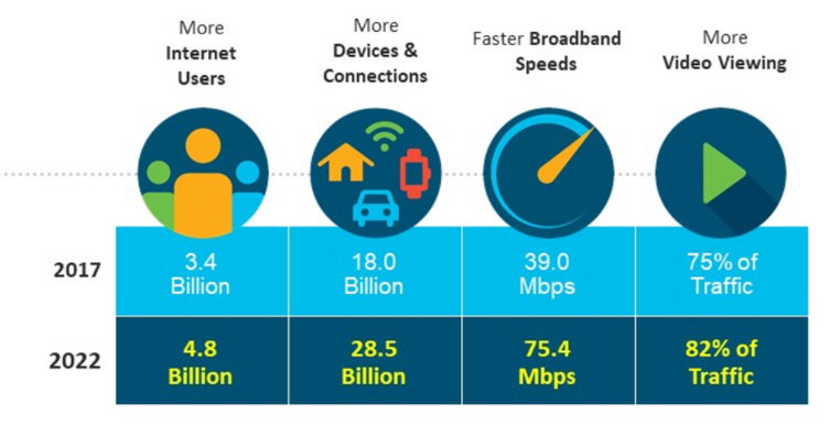
Figure 8. Cisco's latest VNI traffic forecast
3.8x100G solution for 800G SR scenario
a)Application scenario requirement analysis of 800G QSFP-DD or OSFP SR
For 100m data center transmission, the industry has actually been plagued by the VCSEL transmission technology with a rate limit of about 100G per channel, and it seems difficult to continue to lift the speed. The 800G MSA aims to develop low-cost 8x100G QSFP-DD or OSFP optical modules for SR applications, ensuring at least the most important applications in SR, supporting 60 to 100m transmissions, as shown in Figure 9.
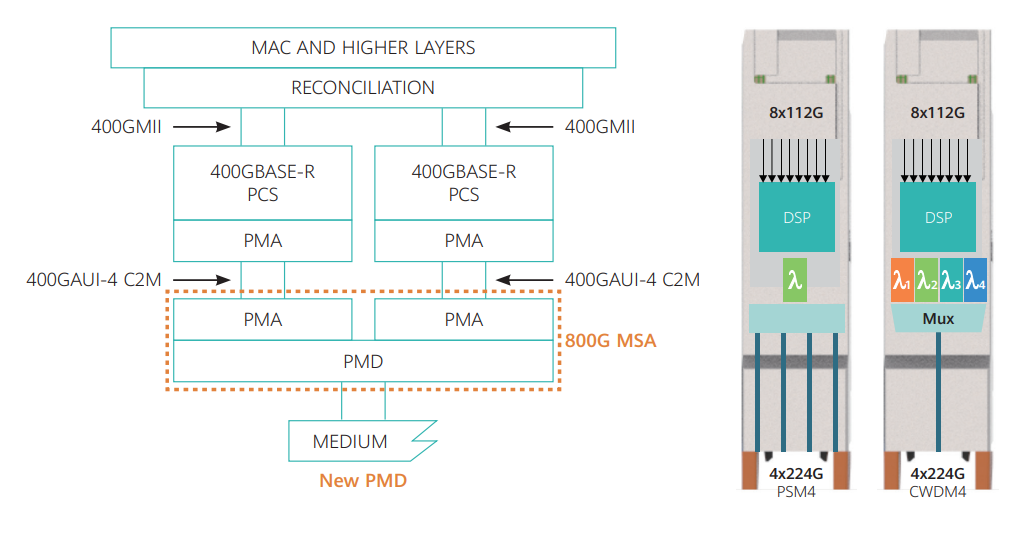
Further, the 800G MSA Working Group is attempting to define a transmitter technology that enables a linear reduction in cost through a highly integrated approach to enable a rapid early push into the 800G high-density optical interconnect market. The low-cost 800G SR8 can support current data center evolutionary trends by providing low-cost serial 100G server connectivity: growing switch ports and decreasing numbers of servers per rack. As shown in Figure 9, the 800G MSA working group will define a low-cost physical medium-dependent sublayer (PMD) specification for single-mode fiber interconnections based on the 100G PAM4 technology. In addition, due to the need for low latency in SR applications, KP4 FEC will be used to implement error correction in 800G MSA optical modules, and other DSP algorithms include simple clock recovery and equalization. A connector will also need to be defined for the PSM8 module to enable connection to 8x100G.
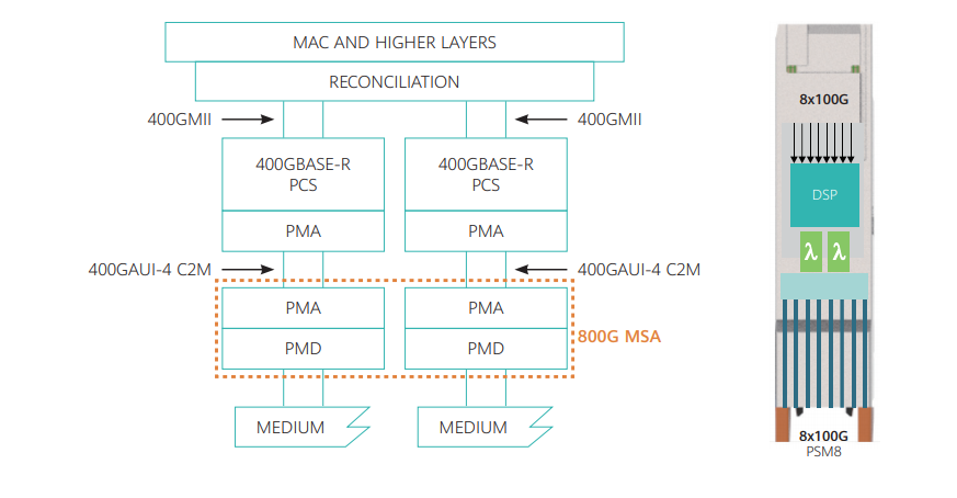
Figure 9. 800G SR8/PSM8 optical module architecture block diagram and 800G MSA specification range
Compared to conventional SR modules, the 800G SR8 will no longer use a VCSEL-based multi-mode solution, but a parallel single-mode transmission method, PSM8, with a modulation format of PAM4 and including a DSP chip.
b) Feasibility analysis of 8x100G solution
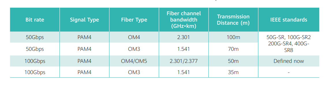
As analyzed above, the single-channel 100G rate may limit the multi-mode solution in 400G QSFP-DD SR8 to continue the evolution to 800G QSFP-DD SR8. Based on IEEE's theoretical model, it can be inferred that when the baud rate reaches the 50G band, the transmission distance supported by multi-mode fiber MMF will not exceed 50m, as shown in Table 3.
The main limiting factors are the modulation bandwidth of VCSEL and the intermodal dispersion of MMF. Although the transmission distance can be extended to about 100m with the help of the powerful DSP algorithm by optimizing the device and optical fiber design, the cost is high cost, with large delay, and power consumption. Based on this, the MSA Pluggable 800G optical Module working group recommends single-mode transmission technology for 800G-SR8 interconnection.
Table 3. The relationship between MMF bandwidth and transmission distance is predicted based on IEEE theoretical model
To ensure a single-mode fiber SMF-based solution with lower cost and power consumption, reasonable PMD standard requirements must be defined for the 800G-SR8. The PMD layer definition needs to satisfy at least three principles:
1) Allow for multiple solution-based transmitter technologies, such as DML, EML, and SiPh.
2) All potential of the device can be fully utilized in order to achieve the target link performance.
3) The parameters of the PMD layer are relaxed as much as possible as long as the reliable link performance is satisfied. These three principles are explained and analyzed in the following with the experimental study results.
First of all, in terms of power budget, the single-mode based 800G-SR8 is expected to be very similar to the 400G-SR8, the only difference being the need to define the insertion loss for the newly defined PSM8 single-mode connector. This means that the DSP chip can meet the power budget requirements of the 800G-SR8 by directly using the proven optoelectronic devices from the current 400G-SR8 interconnect. Therefore, in addition to defining the PSM8 connector, the biggest challenge in defining the 800G-SR8 PMD specification lies in finding the appropriate transmitter optical modulation amplitude (OMA), extinction ratio (ER), transmitter and dispersion eye closure for PAM4 (TDECQ), and receiver sensitivity. To find these suitable metrics, the MSA working group tested and evaluated the BER performance of a number of different transmitters, as shown in Figure 10.
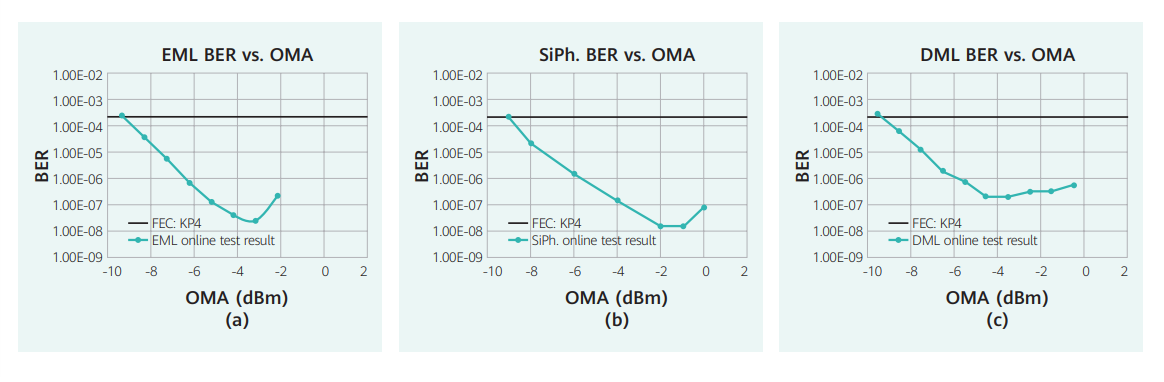
Figure 10. (a) EML BER vs. OMA results based on commercially available 400G DSP ASICs; (b) SiPh BER vs. OMA results based on commercially available 400G DSP ASICs, (c) DML BER vs. OMA results based on commercially available 400G DSP ASICs
The above experimental results are BER vs. OMA curves measured in real-time on a single wavelength 100G PAM4 signal based on a commercial 400G DSP chip. Among them, the 100G results of EML and SiPh may already be known because they have been discussed in recent years, but the sensitivity based on the DML solution is also quite good, only the BER platform is slightly higher, but as long as it is below the BER threshold of KP4 FEC. Since the silicon photonics, optical transmitter loss is a bit larger, its output power is smaller than other solutions, so it needs to try to consider appropriate relaxation when defining the 800G SR8 minimum OMA index.
Note that although DML devices with smaller bandwidth than EML and SiPh devices are used in the above DML results, the use of commercial DSP chips that are more powerful than the IEEE-defined 400GE reference receiver can still achieve better equalization and achieve similar OMA sensitivity as EML and SiPh to meet the 800G SR8 power budget. In order to unleash the full potential of DSP in 800G SR8 applications, receiver compliance tests such as TDECQ need to be redefined to match the actual equalization capability of commercial DSP chips, such as more taps than the currently defined 5 taps.
On the other hand, considering the lower sensitivity requirements in SR scenarios and the strict power consumption constraints in 800G optical modules, the use of low-complexity DSP modes will also be recommended in future 800G optical modules. The extinction ratio ER, as a metric directly related to power consumption, is theoretically the lower the ER the better as long as the reliable transmission of the link is guaranteed. Based on the above analysis, the MSA working group believes that a low-cost, low-power solution based on SMF can be used as a promising solution for 800G-SR applications.
4. 4x200G solution for 800G FR scenario
a) Requirement analysis of 800G FR QSFP-DD or OSFP scenario
Single-channel 200G transmission based on PAM4 modulation technology is the next major technical milestone for Intensity Modulation Direct Detection (IMDD) systems and the foundation for achieving 4-channel 800G optical interconnects, and even further 1.6T high-speed interconnects based on it.
As shown in Figure 11, the working group will define a full set of PMD and partial PMA layer specifications, including a new low-power, low-latency FEC solution for wrapping a layer over the 112G electrical input signal to improve the net coding gain of the modem.
One of the goals of the industry is to develop a new generation of wideband electrical and optical simulators for transmitter and receiver components, including the commonly used ADC and DAC. To meet the power requirements of pluggable 800G optical modules, the next generation of 200G PAM4 DSP chips will be fabricated using a lower junction CMOS process, such as 7nm/5nm, and will also require low-complexity, low-power digital signal processing algorithms to equalize the channel.
Figure 11. 800G FR4/PSM4 optical module structure block diagram and 800G MSA specification range
The 4x200G FR interconnection solution appears to have two realization paths, one is a PSM4 solution with 4 pairs of single-mode fibers, and the other uses a single pair of fibers based on CWDM4, which still has a relatively large difference in external optical port density, and the cost and complexity of CWDM4 modules should also be significantly increased.
b) Feasibility analysis of 4x200G solution
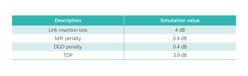
In LAN-WDM, TEC is required for temperature control, while in single-channel 200G application, temperature control is expected to be avoided. The power budget for 800G-FR4 will be analyzed based on CWDM4. The main factors related to the power budget include link insertion loss, multiple path interference (MPI), different group delay (DGD), and transmitter and dispersion penalty (TDP). According to the model published in the IEEE standard, the penalty caused by MPI and DGD is calculated as shown in Table 4. Since the baud of single channel 200G is higher than 100G, the penalty of dispersion must be greater. The Working group recommended a reasonable TDP value of 3.9dB. In summary, taking into account receiver aging, coupling losses, and the optical output power of a typical transmitter, the working group concluded that the sensitivity of the 200G PAM4 receiver needs to be around -5dBm.
Table 4. Power budget analysis of 800G-FR4
Compared to 100G, the baud of 200G doubles, resulting in SNR degradation of 3dB. It may be necessary to use stronger FEC error correction codes to maintain a sensitivity of -5dBm and avoid the BER platform above the Pre FEC BER threshold. Therefore, as mentioned before, an extra layer of low latency and low complexity FEC should be wrapped on top of KP4 FEC when the optical module is implemented. The new FEC error threshold can be set according to the actual optical link performance and power budget requirements.
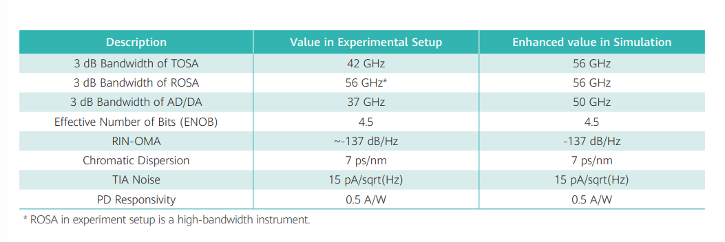
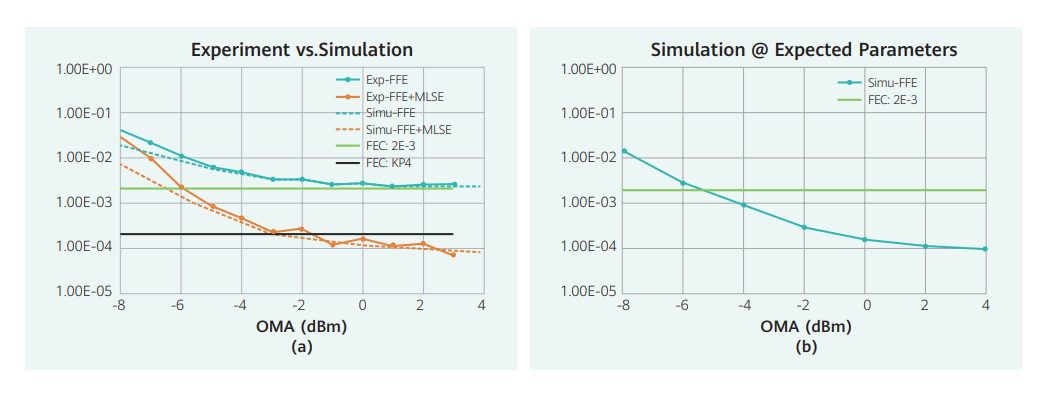
The working group also further analyzed the performance of the single channel 200G link through simulation and experiments. The parameters of the devices used in the link are shown in Table 5. The experimental results show that when the BER threshold of the new FEC is set to 2e-3, the receiver sensitivity can reach the target, as shown in Figure 12(a). However, the maximum likelihood sequence estimation (MLSE) algorithm is used in the experiments to compensate for the strong inter-code interference ISI in the channel due to narrowband filtering.
The dashed line in Figure 12(a) represents the results based on the experimental device parameter simulation. Together with the experimental results, the simulation study shows that the limiting factor for the system performance is the bandwidth of the devices such as DA/AD, driver, and electro-optical modulator. Assuming that high-bandwidth devices will be introduced to the market in the next few years, the simulation is based on the same system but after setting the device bandwidth to a larger size, it is found that the corresponding sensitivity requirement can be met in the DSP at Pre FEC BER=2e-3 using only the forward equalization algorithm (FFE), and the results are shown in Fig. 4(b), which is in accordance with the theoretical expectation.
Table 5. Device parameters used in experiment and simulation
Figure 12. (a) Experimental and simulation results of 200G single channel under the condition of existing device bandwidth; (b) FFE equalization simulation results of 200G single channel with devices with improved bandwidth.
Based on the above analysis, it is still recommended to meet the corresponding TDECQ metrics in the 800G-FR4 scenario compliance test. Only the FFE tap number of reference receivers used in TDECQ testing needs to be increased to an appropriate value, which is also worth further discussion and study. Of course, if the capacity (bandwidth) of future 100Gbd devices falls short of our expectations, we will still have to consider using more complex algorithms such as MLSE in the FR4 scenario, which means developing new compliance solutions.
c) Analysis of 4x200G packaging solution
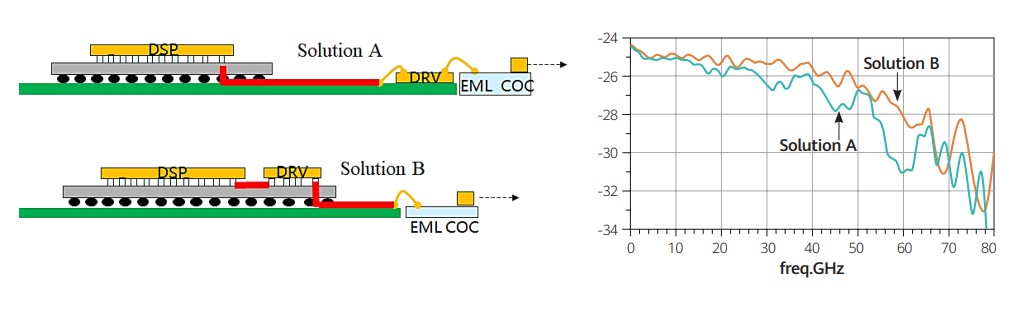
In order to ensure the signal integrity of the high-speed signal considering the Nyquist frequency range (i.e. 56 GHz), the package design of the 4x200G transmitter and the receiver needs to be reconsidered. Two possible implementations of the transmitter are given in Figure 13. Method A is the traditional solution where the Driver and the modulator are placed together. In contrast, the Driver chip designed upside down in solution B is co-packaged with the DSP chip to optimize signal integrity on the RF transmission line. Both of these technologies are currently available.
Preliminary simulation studies show that better results and guaranteed bandwidths greater than 56 GHz can be obtained using solution B. The ripple in the S21 frequency response curve of solution A may be caused by signal reflection on the Driver input, which can be optimized by matching the Driver design to further improve the final performance of solution A.
Figure 13. Two types of packaging for the transmitter. The RF transmission line (red line), alignment, and modulator are considered in the S21 simulation, and the 3 dB bandwidth of the EML chip used is assumed to be 60 GHz.
At the receiver side, the parasitic capacitance needs to be reduced to achieve a high bandwidth photodetector (PD), together with a large bandwidth trans-impedance amplifier (TIA) to ensure the bandwidth of the receiver. There is no technical problem to implement such a device using current semiconductor technology. There are even companies in the industry that have already invested a lot of effort in developing the corresponding products, which are expected to reach mass production within one to two years. In addition, the connection between PD and TIA is also important and needs to be optimized and analyzed because parasitic effects can affect performance.
d) Forward Error Correction Coding (FEC) in single channel 200G
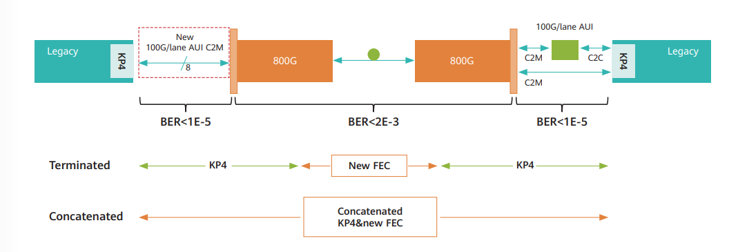
Overall, a stronger FEC solution with a PreFEC BER threshold of 2e-3 has been mentioned previously to ensure the sensitivity requirements of the 200G PAM4 receiver. Figure 14 shows the results of the comparison between cascading and replacement solutions. In the first solution, the KP4 FEC is replaced with the new, more expensive FEC at the intermediate optical port, which has advantages in terms of total overhead and net coding gain. In the second solution, a cascaded FEC approach is adopted, where KP4 continues to be retained as the outer coding layer and is used in conjunction with the new inner code. This cascaded code has the benefit of low latency and power consumption and thus is more suitable for the 800G-FR4 application scenario.
Figure 15. 800G FEC solution: New Replacement FEC vs Cascaded KP4 FEC
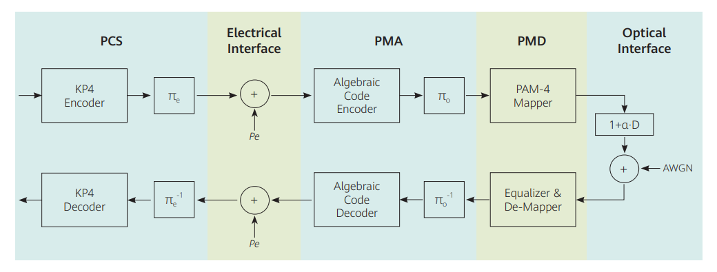
A more direct way to achieve 2E-3 BER threshold FEC is to connect the generation numbers shown in Figure 16 in series with KP4, minimizing power consumption and end-to-end delay. Both Hamming codes with single BER correction capability and BCH codes with double BER correction capability are suitable choices for the generation codes in this cascade scheme. Both internal codes have an overhead of about 6% and combined with a simple soft-in-hard-out (SIHO) recursive decoding algorithm with 64 test Patterns, both Hamming and BCH codes can achieve better than 2e-3 threshold error correction performance. The symbol distribution defined in 400GBASE-R essentially serves as a parity interleaver for cascaded coding, and the 10k bit delay is sufficient for de-correlation with noise introduced in the fiber.
Figure 16. Structure diagram of cascade scheme for KP4 and linear codes
5. Possible solutions for 800G DR QSFP-DD or OSFP scenarios
As shown in Table 6, there are four paths to achieve 800G DR.
First, the SR8 solution defined in the 800G MSA can directly extend the transmission range by 500m. Since the parallel fiber solution requires more fibers, the cost of fibers up to 500m long may be an issue in this application.
Second, based on the existing FR4 solution, a 2x400G CWDM solution can be provided by simply doubling the transceiver devices, which seems to strike a good balance of fiber resource consumption and scheme maturity, but it is cost and power consumption may limit its practical application.
Finally, the next generation of single-channel 200G solutions (PSM4 or CWDM4) may be able to cover DR applications. This approach requires only 4 pairs of optical transceiver modules and appears to have the lowest power consumption and cost. However, due to the maturity of the industry and the practical feasibility of further proof, it is not clear when the solution will be commercially available.
Table 6. Four possible solutions for 800G DR
In summary, four possible options for 800G DR Have been discussed and the Working Group will continue to monitor the development of each technical route and recommend options at an appropriate time in the future.
6. Summary and Outlook
The 800G pluggable MSA will take the lead in defining optical modules for both 800G-SR8 and FR4 scenarios. In the SR8 scenario, in order to take more technologies into account and introduce SMF-based single-mode solutions, the working group considered appropriate adjustments to some key parameters of the PMD layer, eventually allowing the OMA and ER requirements to be relaxed to reduce power consumption, and the reference receivers for TDECQ testing will need to be redefined.
The working group also demonstrated the technical feasibility of single-channel 200G optical transmission for 800G FR4 applications. Experimental and simulation results showed that it is necessary to add a low-latency and low-power FEC coding sublayer in the optical module to achieve the target power budget. Technical details of this new FEC will be presented in the 800G-FR4 standard specification to facilitate multi-vendor interoperability. At the same time, device bandwidth enhancement and module package design optimization are two issues that need further study.
The 800G pluggable MSA released the first version of the specification in Q4 2020, with a small number of devices already in prototype and the first 800G optical models expected to be available in 2021. With the 400GbE generation ready to be rolled out in the market, 800G pluggable optical modules will leverage the new ecosystem to provide higher interconnect density for the next generation of 25.6T and 51.2T switches to enabling cost-effective single-channel 100G and 200G optical interconnects.
Looking beyond 800G to 1.6T, the industry is beginning to see the possible limitations of pluggable optical modules. Using classic PCBs, SerDes for C2M interconnects are unlikely to scale to single-channel 200G rates, requiring analog electronics/chips and optical devices to be placed closer to the switching chip. Whether the industry will eventually choose co-packaged optics (CPO), or on board optics (OBO), or an upgraded version of pluggable, the MSA definition of single-channel 200G will be 800G and 1.6T interconnect the necessary base unit, the importance, and significance of self-evident.


 PAM4 CWDM Duplex LC 2km SMF Optical Transceiver Module")
 PAM4 1291/1311nm 2km DOM Duplex LC SMF Optical Transceiver Module")
 PAM4 1291/1311nm 2km DOM Dual CS SMF Optical Transceiver Module")
 PAM4 1311nm MPO-12 500m SMF DDM Optical Transceiver Module")
 PAM4 CWDM 2km DOM Duplex LC SMF Optical Transceiver Module")
 2km 1291/1311nm Dual Duplex LC SMF Transceivers")
 2km 1291/1311nm Dual CS SMF Transceivers")
 1311nm 500m Dual MPO-12 SMF Transceivers")


