Introduction
With the rapid development of AI and HPC technology, the high-speed interconnect and scalability of GPUs have put forward higher requirements, a high-bandwidth, low-latency, high-performance interconnect technology is critical to the overall AI computing performance improvement. In April this year, Lao Huang proposed the third generation of NVIDIA NVSwitch and the fourth generation of NVLink technology at the GTC conference, which provides a high-speed point-to-point interconnection solution for the newly released H100 GPUs that is even faster than the A100 GPUs, and this kind of network has the prototype of the NVLink network.
The third-generation NVSwitch chip, referred to as NVSwitch3, can be used to connect each GPU card inside the server and extend the GPU server’s external connection to establish a complete independent GPU high-speed cluster. At the same time, the NVSwitch chip supports multicast message acceleration through hardware gas pedals and introduces SHARP (Scalable Hierarchical Aggregation and Reduction Protocol), which is an important feature only available in IB switches before and is mainly used to accelerate and optimize the All-Reduce AI computation. -Reduce AI computing performance. Meanwhile, through the third-generation NVSwitch chip composed of physical switches, it is possible to build a cluster of up to 256 H100 GPU cards, and the whole network provides 57.6TB/s of all-to-all bandwidth. The NVLink 4.0 specification it adopts can greatly optimize GPU performance and scalability, such as the parallel process block structure of the GPU architecture echoes the parallel structure of NVLink, while NVLink’s interface is further optimized for the exchange of data in the GPU L2 cache.
NVLink
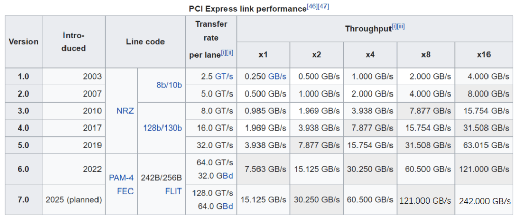
NVLink is a protocol to solve the point-to-point communication between GPUs within the server, the traditional PCIe Switch rate is as follows, the latest PCIE5.0 is only 32Gbps bandwidth per lane, which basically does not satisfy the communication bandwidth requirements between the GPUs, and with NVLink technology, the GPUs can be directly in the server-internal With NVLink technology, GPUs can directly interconnect with each other within the server at high speeds, without the need to communicate via PCIe switches. The fourth-generation NVLink has 112Gbps bandwidth per lane, which is three times higher than the bandwidth of a PCIe Gen5 lane.
The main purpose of NVLink is to provide a high-speed, point-to-point network for GPU interconnections without the overhead of end-to-end message retransmission, adaptive routing, and message reassembly compared to traditional networks. The extremely simplified NVLink interface provides CUDA acceleration from the session layer to the representation layer, to the application layer, thus further reducing network overhead due to communication.
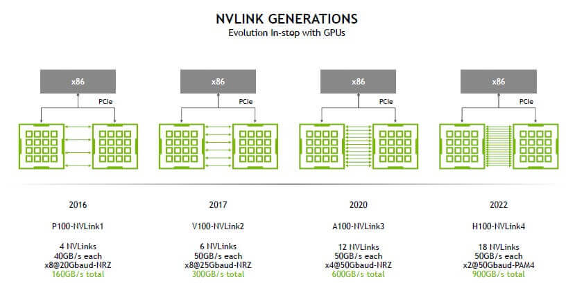
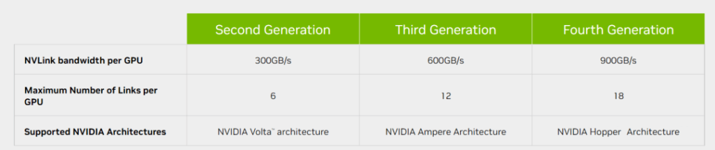
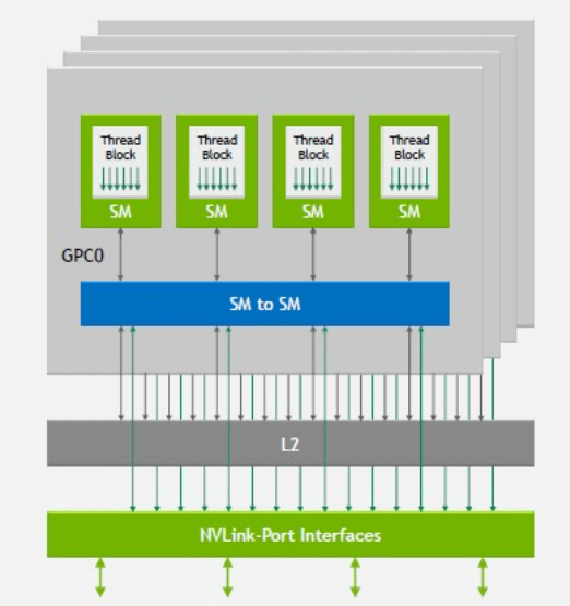
As shown in the figure, we can see that NVLink has evolved along with the GPU architecture, from the first-generation NVLink1 for P100 to the current NVLink4 for H100. NVLink3 supports both 50G NRZ and 56G PAM4, while NVLink4 introduces 112G PAM4 Serdes for the first time, which can provide 900GB/s of bidirectional bandwidth, a 1.5x increase over the previous generation NVLink3’s 600GB/s. So how is 900GB/s calculated? Each H100 GPU is connected to an internal NVSwitch3 chip via 18 NVLink4 links, and each NVLink4 link is actually two lanes, each lane is 112G PAM4, so a single NVLink4 link has a unidirectional bandwidth of 224Gbps, or 25GB/s (note that here it changes from bits to Byte) unidirectional bandwidth, 50GB/s bidirectional bandwidth, and 18 NVLink4 links have a total of 900GB/s bidirectional bandwidth.
NVSwitch Chip
An NVSwitch chip is a type of switch ASIC that can link multiple GPUs with high-speed NVLink interfaces, enhancing the communication and bandwidth among GPUs within a server. When P100 used NVLink1, there was no NVSwitch chip and the GPUs formed a ring connection, which prevented direct communication between GPUs on different NUMA nodes. Starting from V100 with NVLink2, an NVSwitch1 chip was added, and then A100 with NVLink3 used the NVSwitch2 chip. The next one is the NVSwith3 chip for H100.
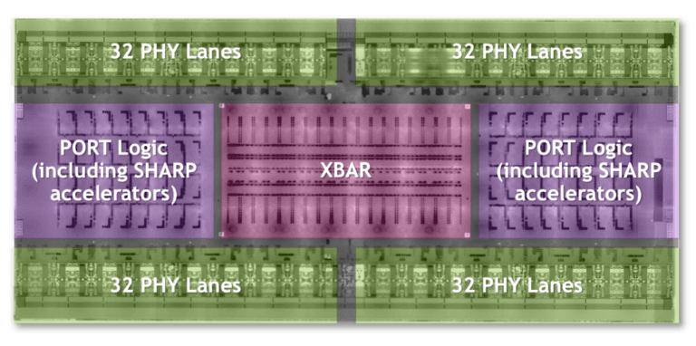
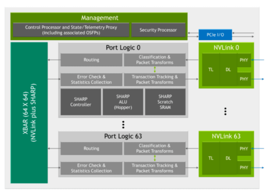
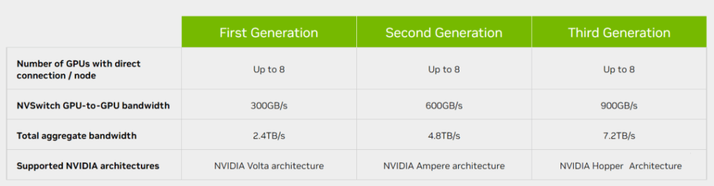
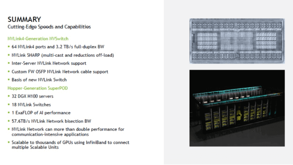
The chip is fabricated with TSMC’s 4N process and packs 25.1 billion transistors on a die of 294 square millimeters. The chip measures 50mm by 50mm and features a SHARP controller that can handle 128 SHARP parallel groups simultaneously. It also has a SHARP ALU embedded in it, which can perform logic operations on the data stored in the SRAM memory that supports SHARP computation. The SHARP ALU enables NVSwitch to achieve 400GFLOPS of FP32 computing throughput, and it also supports various precision modes such as FP16, FP32, FP64, and BF16. The chip can interface with either 400Gbps Ethernet or NDR IB connections through its PHY circuit, and each cage can accommodate four NVLink4 OSFP optical modules with FEC capability. The chip has security features that allow partitioning of the NVLink network into subnets, as well as telemetry monitoring functions similar to IB. The NVSwitch3 chip has 64 NVLink4 ports, each with two lanes that deliver 200Gbps of unidirectional bandwidth. Therefore, the chip can offer a total of 64*200Gbps=12.8Tbps of unidirectional bandwidth or 3.2TB/s of bidirectional bandwidth.
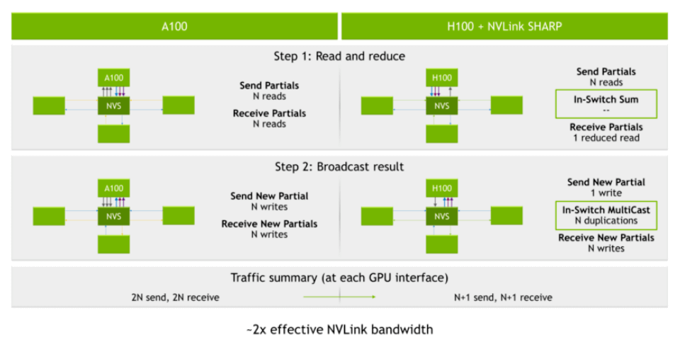
NVSwitch3 chip is the first to integrate the entire SHARP function, which uses hardware to aggregate and update the computation results of multiple GPU units during all reduce, thereby reducing the number of network packets and improving computational performance.
NVLink server
NVLink server refers to a server that uses NVLink and NVSwitch technology to interconnect GPUs, usually NVIDIA’s own DGX series servers, or OEM HGX servers with similar architectures.
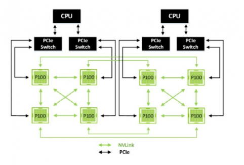
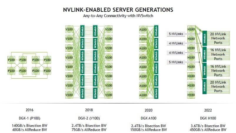
The DGX-1 server with P100 GPUs did not introduce NVSwitch, and all 8 GPUs were connected by NVLink1, with each P100 having 4 NVLink1 connections. The NVSwitch1 and NVLink2 were introduced in the NVIDIA V100 GPU architecture, providing high bandwidth and any-to-any connection between multiple GPUs within a server. The NVSwitch2 and NVLink3 were launched in the NVIDIA A100 GPU.
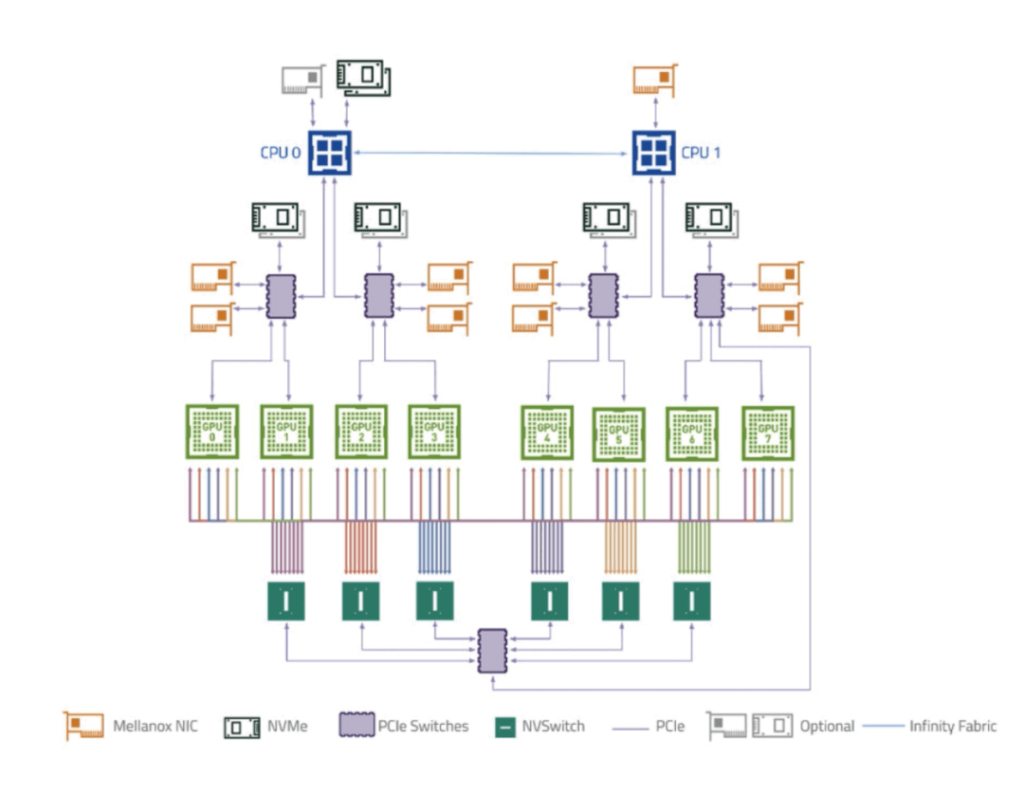
In the above DGX A100 server-internal diagram, the connection between GPU and CPU is through PCIe Switch, and the connection between 8 GPUs is mainly through 6 NVSwitch2 chips. Each GPU connects to the NVSwitch2 chip with 12 NVlink3, and each NVlink3 has 25GB unidirectional bandwidth, which can provide a total of 12*25GB=300GB/s unidirectional bandwidth or 600GB/s bidirectional bandwidth for a GPU. Let’s take a look at the DGX H100 server parameters:
- 8x NVIDIA H100 Tensor Core GPUs with 640GB of aggregate GPU memory
- 4x third-generation NVIDIA NVSwitch chips
- 18x NVLink Network OSFPs
- 3.6 TB/s of full-duplex NVLink Network bandwidth provided by 72 NVLinks
- 8x NVIDIA ConnectX-7 Ethernet/InfiniBand ports
- 2x dual-port BlueField-3 DPUs
- Dual Sapphire Rapids CPUs
- Support for PCIe Gen 5
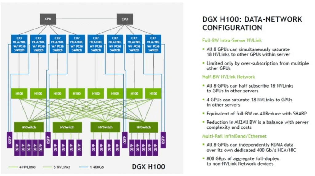
The H100 GPU introduced the third-generation NVSwitch and the fourth-generation NVLink technology, which can provide a unidirectional bandwidth of 450GB/s for a single H100 GPU. It also introduced an external 1U box-type NVLink Switch switch, which provides high-speed communication for multiple GPU servers. There are 8 H100 GPUs in the DGX H100, and each H100 is connected to 4 NVSwitch3 chips with 18 NVLinks (5,4,4,5) at the same time. The traffic between GPUs is distributed to 4 switching planes, thereby achieving all-to-all traffic within the GPU. Each internal NVSwitch3 chip has a 2:1 convergence ratio for the external NVLink, mainly designed to consider the complexity and cost of inter-server connection bandwidth.
NVSwitch
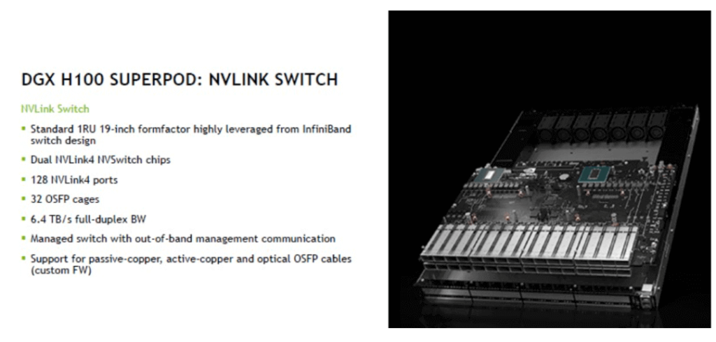
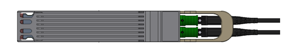
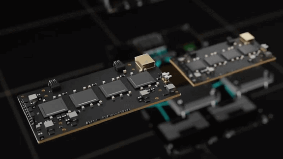
The NVLlink switch was just released this year and was born for the interconnection of the H100 Superpod. It adopts a 1U size design with 32 OSFP ports, each OSFP comprises 8 112G PAM4 lanes, and each switch has 2 built-in NVSwitch3 chips. Each NVSwitch3 has 64 NVLink4s, so two chips can provide up to 128 NVLink4 interfaces, providing 128*400Gbps =51.2TBps unidirectional bandwidth, or 6.4TB/s bidirectional bandwidth. The NVLink switch supports out-of-band management ports, DAC cables, and AOC and OSFP cables with specific firmware. There is no public information about this OSFP module yet. The appearance is guessed to be similar to the NDR OSFP shape below. Two MPO ports each connect a 400G or directly connect an 800G port to a 24-core MPO cable.
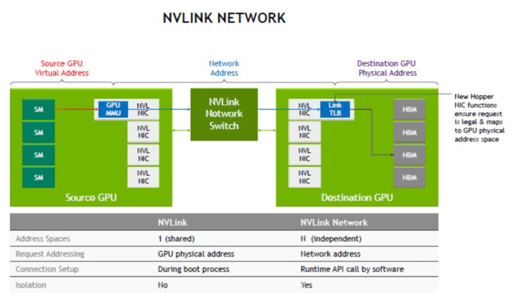
NVLink Network
With the NVSwitch physical switch, we can connect multiple NVLink GPU servers into a large Fabric network, which is the NVLink network. This network is mainly designed to solve the high-speed communication bandwidth and efficiency problems between GPUs and does not include the computation network and storage network between CPUs. In the era without the NVLink network, each server allocates local address space for GPUs internally and then communicates with each other through NVLink. In the NVLink network, each server has its own independent address space, which is used to provide data transmission, isolation, and security protection for GPUs in the NVLink network. When the system starts, the NVLink network automatically establishes connections through software APIs and can change addresses at any time during operation.
The following figure compares the NVLink network and the traditional Ethernet network. It can be seen that through NVlink, NVSwitch chip and NVSwitch switch, an NVLink network that is independent of IP Ethernet and dedicated to GPU service can be formed.
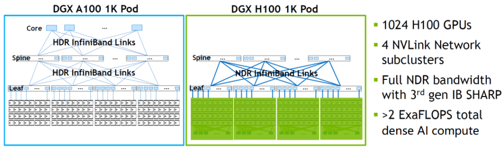
DGX H100 SuperPOD
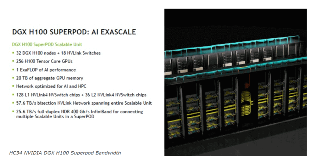
A SuperPOD consists of eight racks, each with four DGX H100 servers, for a total of 32 servers and 256 H100 GPU cards, delivering 1 exaFLOP (one quintillion) of FP8 precision sparse AI performance. The NVLink network within this SuperPOD can provide a total of 57.6TB/s all-to-all bidirectional bandwidth for 256 GPUs, while the CX7 inside the 32 DGX H100 servers can interconnect with the IB switch, providing 25.6TB/s of bidirectional bandwidth, which allows using or connecting multiple SuperPODs within a POD.
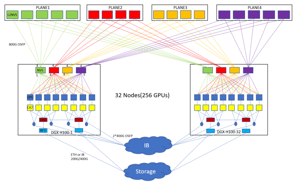
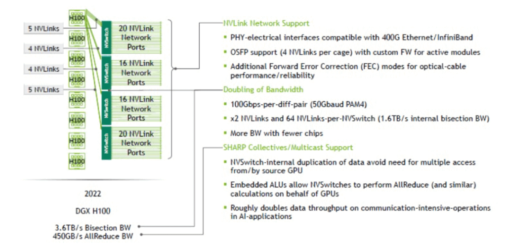
NVS is the NVSwitch3 chip mentioned earlier, and L2NVS is the NVSwitch physical switch mentioned earlier. Each GPU in a DGX H100 extends 18 NVLink4 connections northward, providing 1850GB=900GB/s bidirectional bandwidth. These 18 NVLink4 are divided into four groups of 5,4,4,5 and connected to four onboard NVSwitch3 chips. In this way, for 8 GPUs, each NVS chip connects 40,32,32,40 NVLink4 southward, for a total of 114 NVLink4, and then each NVS chip does a 2:1 convergence, connecting 4,4,4,4 NVLink4 northward to the external 18 L2NVS, which are the NVSwitch 1U switches we mentioned earlier. These switches are divided into four groups of 5,4,4,5. Thus, a single onboard NVS chip connects 20,16,16,20 NVLink4 northward, for a total of 72 NVLink4, and 114 NVLlink4 southward, forming a 2:1 convergence ratio. Here each NVLink4 consists of two 112G PAM4 lanes, so every four NVLink links require a pair of 800G OSFP modules to connect end-to-end. In this way, the upper half of the figure shows a high-speed network of GPU all-to-all interconnection that forms an NVlink network.
The video below shows how to use 800G OSFP SR8 on NVIDIA Quantum-2 switches.
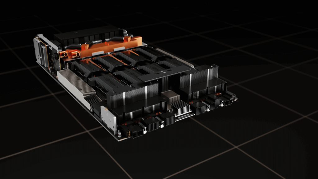
The interconnection between the GPU and CPU is through the PCIe GEN5 Switch inside the CX7 network card. The CX7 network card inside the DGX H100 is not in the form of eight independent CX6 network cards as in the previous DGX A100 but is made into two boards with network card chips to plug into the server. Each of the four CX7 chips forms a Cedar board and outputs two 800G OSFP ports. Eight CX7 network card chips form two Cedar boards and output a total of four OSFP 800G ports. This provides 800Gbps4*2=800GB/s bidirectional bandwidth. The CX7 network card here can run RoCE in Ethernet mode or run in the NDR IB network. As shown in the figure below, 1024 GPUs in four H100 SuperPODs can be built with NDR IB’s fat-tree topology.
Each DGX H100 also has two Bluefield 3s to connect to the storage network.
InfiniBand Network VS NVLink Network
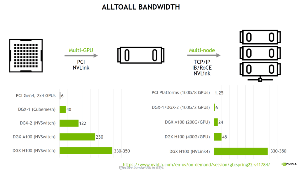
How much faster will the H100 GPU’s connection be after using the NVLink network, compared to the A100’s IB network? Here is a bandwidth comparison between the DGX A100 256 POD and the DGX H100 256 POD:
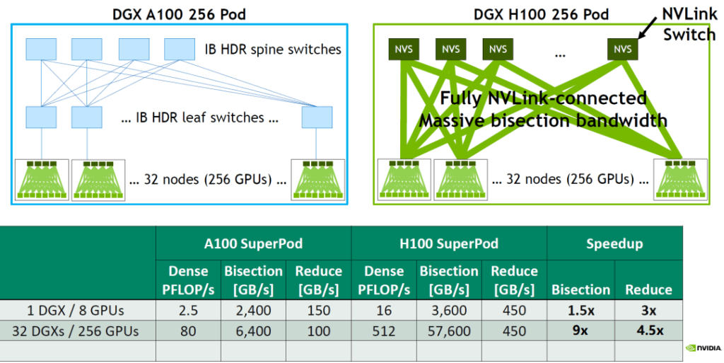
Bisection is a performance indicator of how much data each GPU needs to send to all other GPUs simultaneously in an all-to-all scenario. It usually calculates the network bandwidth when half of the nodes in the network send data to the other half, and it generally measures 1:1 non-blocking traffic. 1 DGX A100 internal: 8/2600GB/s=2400GB/s 32 DGX A100 internal, a total of 256 A100 GPUs, each server connected by 8 200Gbps HDR cards, and the TOR switch should have a 4:1 convergence ratio: 256/2/4200GB/s=6400GB/s 1 DGX H100 internal: 8/2900GB/s=3600GB/s 32 DGX H100 internal, the network convergence ratio is 2:1, so: 256/2/2900GB/s=57600GB/s (which is where the previous mention of 57.6TB/s comes from) The Bisection of a single DGX can increase the bandwidth by 1.5 times and the bidirectional bandwidth by 3 times, and the Bisection of 32 DGX can increase the bandwidth by 9 times and the bidirectional bandwidth by 4.5 times.
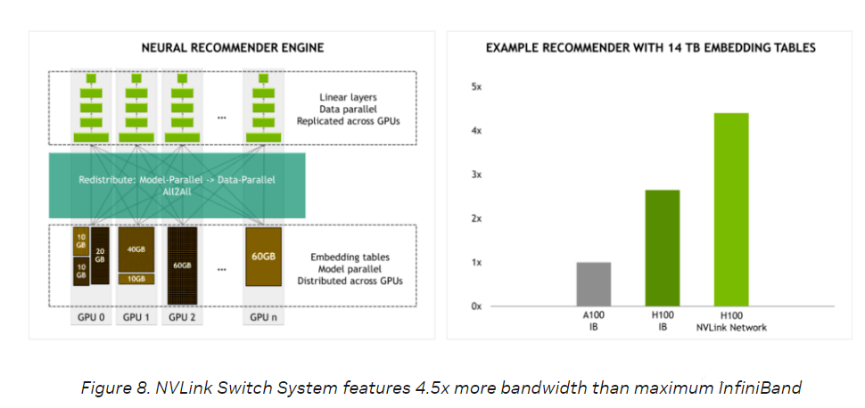
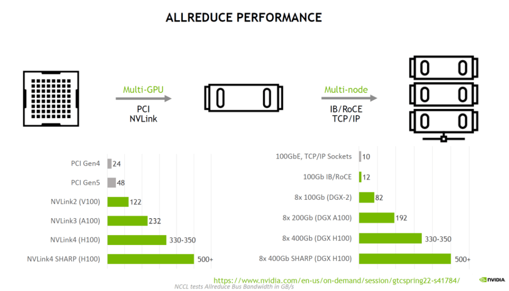
As shown in the figure, for training a recommendation system with a 14TB embedding table running on the all2all data model, the H100 with NVLink has higher performance than the H100 with IB. The following are the public NCCL results of the all-reduce and all-to-all bandwidth comparison for multi-GPU and multi-node GPU running on the server. By optimizing NVLink4 and NVSwitch3, the H100 can achieve consistent bandwidth for internal and external multi-cards.
Conclusion
NVlink and NVSwitch technologies are developed to meet the needs of high-speed, low-latency point-to-point and point-to-multipoint communication for multi-GPU. They are also constantly innovating with the changes in GPU architectures. Since acquiring Mellanox, NVIDIA has also started to combine NVLink technology and IB technology, launching a new generation of NVSwitch chips and switches with SHARP functions, which are optimized for GPU server external networks. The current NVLink network scale that supports up to 256 GPUs is just the beginning. It is believed that this NVlink network scale will further develop and improve in the future, and perhaps create a supercomputing cluster suitable for AI computing, CPU computing, storage, and other network integration.
Related Products:
-
 NVIDIA MMA4Z00-NS400 Compatible 400G OSFP SR4 Flat Top PAM4 850nm 30m on OM3/50m on OM4 MTP/MPO-12 Multimode FEC Optical Transceiver Module
$550.00
NVIDIA MMA4Z00-NS400 Compatible 400G OSFP SR4 Flat Top PAM4 850nm 30m on OM3/50m on OM4 MTP/MPO-12 Multimode FEC Optical Transceiver Module
$550.00
-
NVIDIA MMA4Z00-NS-FLT Compatible 800Gb/s Twin-port OSFP 2x400G SR8 PAM4 850nm 100m DOM Dual MPO-12 MMF Optical Transceiver Module
$650.00
-
NVIDIA MMA4Z00-NS Compatible 800Gb/s Twin-port OSFP 2x400G SR8 PAM4 850nm 100m DOM Dual MPO-12 MMF Optical Transceiver Module
$650.00
-
NVIDIA MMS4X00-NM Compatible 800Gb/s Twin-port OSFP 2x400G PAM4 1310nm 500m DOM Dual MTP/MPO-12 SMF Optical Transceiver Module
$900.00
-
NVIDIA MMS4X00-NM-FLT Compatible 800G Twin-port OSFP 2x400G Flat Top PAM4 1310nm 500m DOM Dual MTP/MPO-12 SMF Optical Transceiver Module
$1199.00
-
NVIDIA MMS4X00-NS400 Compatible 400G OSFP DR4 Flat Top PAM4 1310nm MTP/MPO-12 500m SMF FEC Optical Transceiver Module
$700.00
-
NVIDIA(Mellanox) MMA1T00-HS Compatible 200G Infiniband HDR QSFP56 SR4 850nm 100m MPO-12 APC OM3/OM4 FEC PAM4 Optical Transceiver Module
$139.00
-
NVIDIA MFP7E10-N010 Compatible 10m (33ft) 8 Fibers Low Insertion Loss Female to Female MPO Trunk Cable Polarity B APC to APC LSZH Multimode OM3 50/125
$47.00
-
NVIDIA MCP7Y00-N003-FLT Compatible 3m (10ft) 800G Twin-port OSFP to 2x400G Flat Top OSFP InfiniBand NDR Breakout DAC
$260.00
-
NVIDIA MCP7Y70-H002 Compatible 2m (7ft) 400G Twin-port 2x200G OSFP to 4x100G QSFP56 Passive Breakout Direct Attach Copper Cable
$155.00
-
NVIDIA MCA4J80-N003-FTF Compatible 3m (10ft) 800G Twin-port 2x400G OSFP to 2x400G OSFP InfiniBand NDR Active Copper Cable, Flat top on one end and Finned top on other
$600.00
-
NVIDIA MCP7Y10-N002 Compatible 2m (7ft) 800G InfiniBand NDR Twin-port OSFP to 2x400G QSFP112 Breakout DAC
$190.00