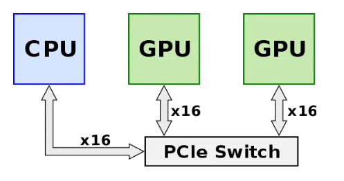
NVLink is a technology developed by NVIDIA for point-to-point high-speed interconnection between GPUs. It aims to overcome the bandwidth limitation of PCIe interconnection and enable low-latency, high-bandwidth data communication among GPU chips, allowing them to work together more efficiently. Before NVLink technology was introduced (before 2014), GPUs had to be interconnected through a PCIe switch, as shown in the figure below. The signal from the GPU had to pass through the PCIe switch first, where data processing involved CPU distribution and scheduling, which added extra network latency and limited system performance. At that time, the PCIe protocol had reached Gen 3, with a single-channel rate of 8Gb/s and a total bandwidth of 16GB/s (128Gbps, 1 Byte= 8 bits) for 16 channels. As GPU chip performance improved continuously, its interconnection bandwidth became a bottleneck.
Source: https://en.wikichip.org/wiki/nvidia/nvlink
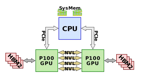
In 2014, NVLink 1.0 was released and applied to the P100 chip, as shown in the following figure. There are four NVlinks between two GPUs, each link containing eight lanes, each with a rate of 20Gb/s. Therefore, the bidirectional bandwidth of the whole system is 160GB/s, which is five times that of PCIe3 x16.
Source: https://en.wikichip.org/wiki/nvidia/nvlink
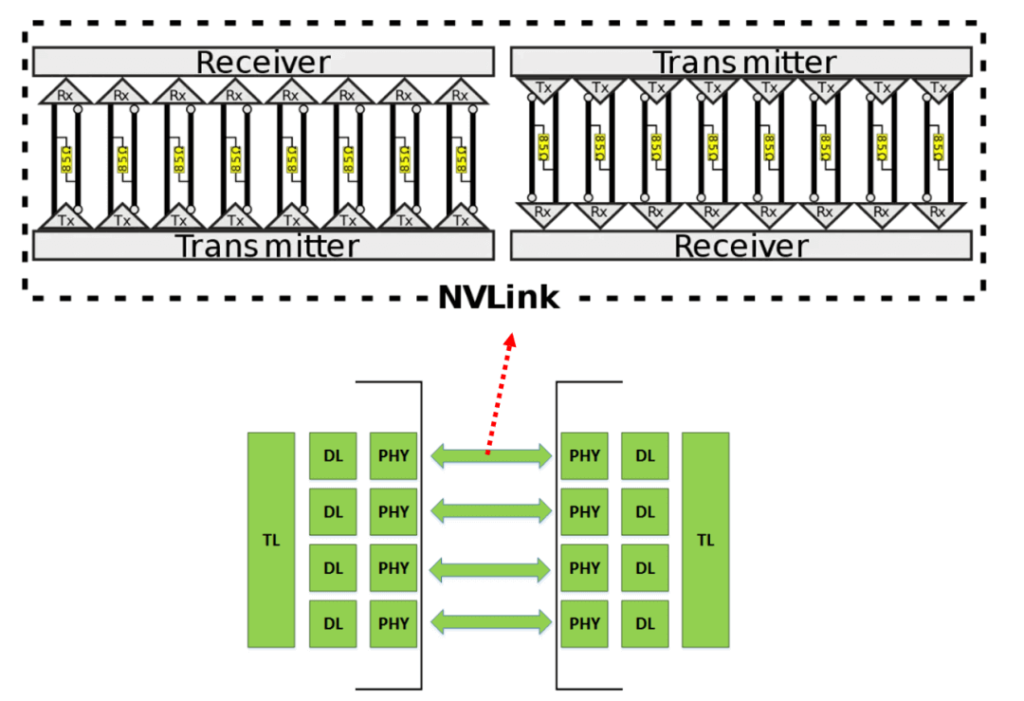
Each NVLink consists of 16 pairs of differential lines, corresponding to eight lanes of channels in both directions, as shown in the following figure. The two ends of the differential pair are PHYs, which contain SerDes.
Source: https://www.nextplatform.com/2016/05/04/nvlink-takes-gpu-acceleration-next-level/
Based on NVLink 1.0, a planar mesh structure of four GPUs can be formed, with point-to-point connections between each pair. Eight GPUs correspond to a cube-mesh, which can form a DGX-1 server. This also corresponds to the common eight-card configuration, as shown in the following figure. It should be noted that at this time, the eight GPUs do not form an all-to-all connection.
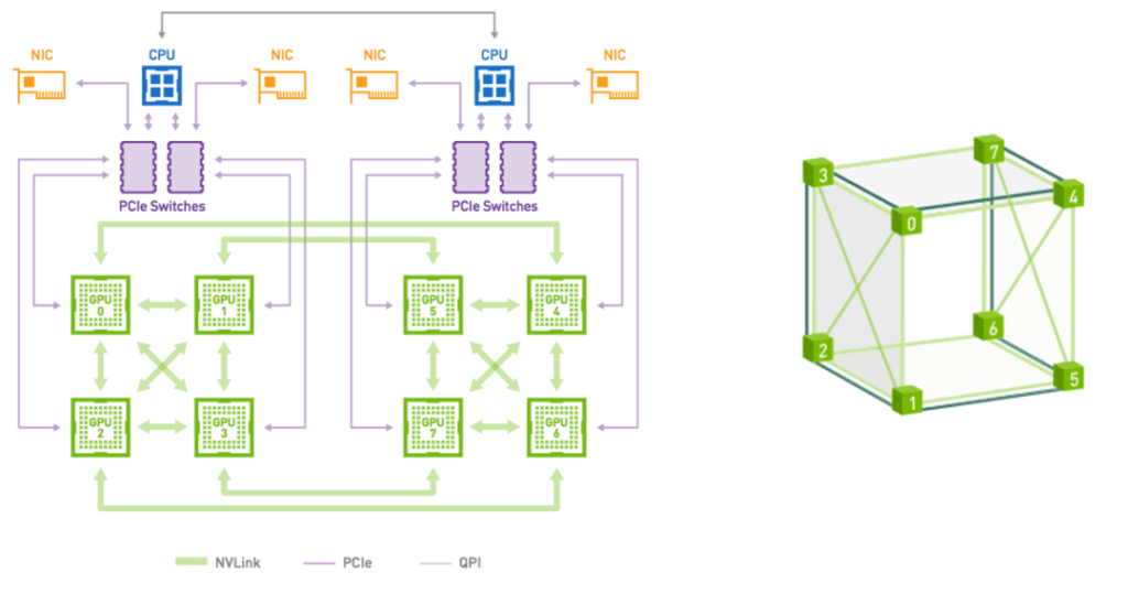
Source: https://developer.nvidia.com/blog/dgx-1-fastest-deep-learning-system/
In 2017, Nvidia launched the second generation of NVLink technology. It connects two GPU V100 chips with six NVLinks, each consisting of eight lanes. The rate of each lane is enhanced to 25Gb/s, and the system’s bidirectional bandwidth reaches 300GB/s, almost double that of NVLink 1.0. Simultaneously, to enable all-to-all interconnection among eight GPUs, Nvidia introduced the NVSwitch technology. NVSwitch 1.0 has 18 ports, each with a bandwidth of 50GB/s, and a total bandwidth of 900GB/s. Each NVSwitch reserves two ports for connecting to the CPU. Using six NVSwitches, an all-to-all connection of eight GPU V100 chips can be established, as illustrated in the figure below.
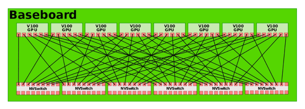
Source: https://en.wikichip.org/wiki/nvidia/nvswitch
The DGX-2 system comprises two boards as shown in the figure below, achieving an all-to-all connection of 16 GPU chips.
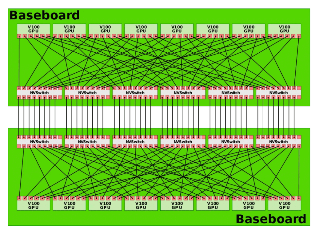
Source: https://en.wikichip.org/wiki/nvidia/nvswitch
In 2020, NVLink 3.0 technology emerged. It links two GPU A100 chips with 12 NVLinks, each containing four lanes. The speed of each lane is 50Gb/s, and the bidirectional bandwidth of the system reaches 600GB/s, which is double that of NVLink 2.0. As the number of NVLinks increased, the number of ports on the NVSwitch also rose to 36, each with a rate of 50GB/s. The DGX A100 is composed of eight GPU A100 chips and four NVSwitches, as illustrated in the figure below.
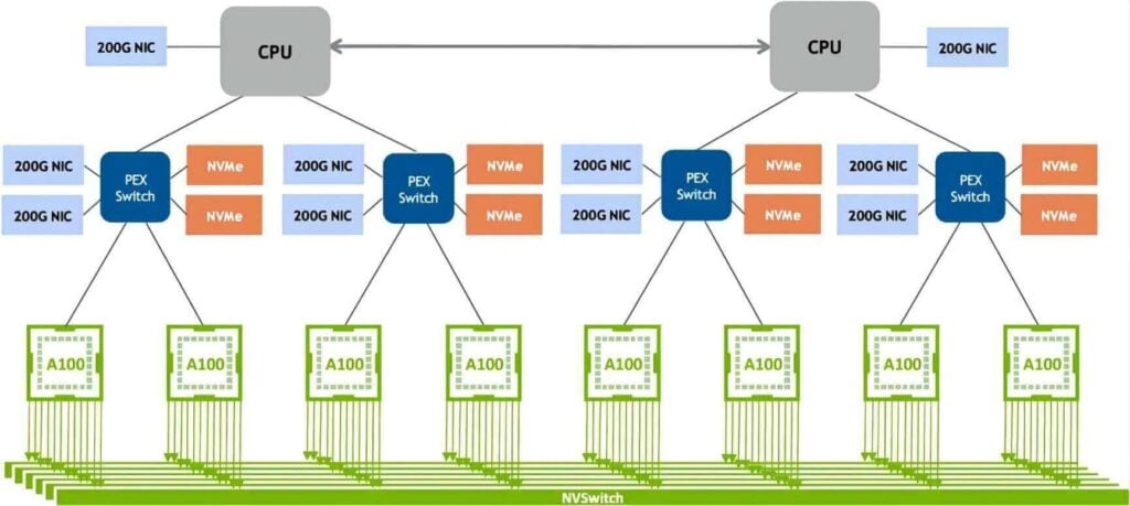
Source: http://www.eventdrive.co.kr/2020/azwell/DGX_A100_Azwellplus.pdf
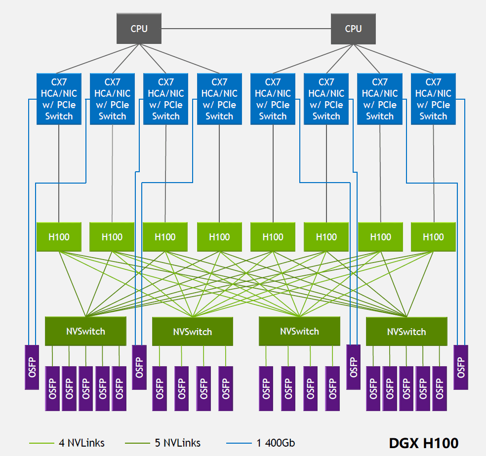
In 2022, NVLink technology was upgraded to the fourth generation, which allows two GPU H100 chips to interconnect through 18 NVLink links, each link containing 2 lanes, each lane supporting a rate of 100Gb/s PAM4, thus the bidirectional total bandwidth increased to 900GB/s. NVSwitch was also upgraded to the third generation, each NVSwitch supporting 64 ports, each port with a rate of 50GB/s. DGX H100 consists of 8 H100 chips and 4 NVSwitch chips, as shown in the figure below. On the other side of each NVSwitch, multiple 800G OSFP optical modules are connected. Taking the first NVSwitch on the left as an example, its unidirectional total bandwidth on the side connected to the GPU is 4Tbps (20NVLink200Gbps), and the total bandwidth on the side connected to the optical module is also 4Tbps (5800Gbps), both of which are equal in size, forming a non-blocking network. It should be noted that the bandwidth in the optical module is unidirectional bandwidth, while in AI chips, bidirectional bandwidth is generally used.
Source: https://blog.apnic.net/2023/08/10/large-language-models-the-hardware-connection/
The 800G OSFP SR8 optical transceiver module is designed for 400G InfiniBand NDR links over multimode fiber using 850nm wavelength. The module has two ports of 4-channel 100G-PAM4 optical modulation, each using an MTP/MPO-12 connector. In the below video, you will see how to connect it to another device using breakout fiber cables, and how to configure the switch protocol based on InfiniBand or Ethernet. You will also learn about the key features and benefits of the 800G OSFP SR8 module, such as its high bandwidth, low power consumption, and hot pluggability.
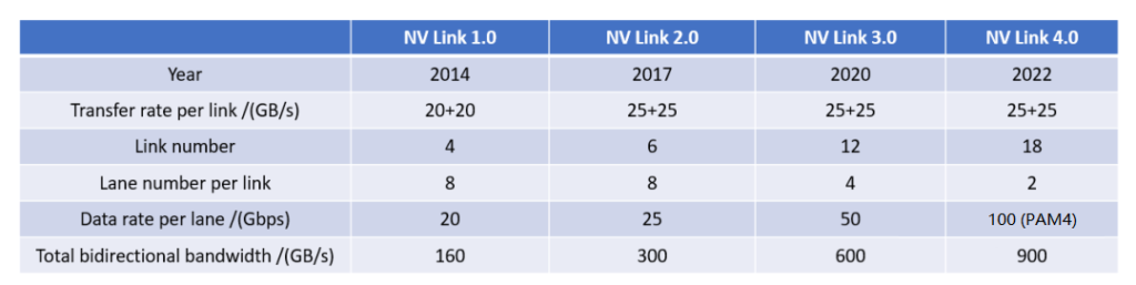
The following table summarizes the performance parameters of each generation of NVLink.
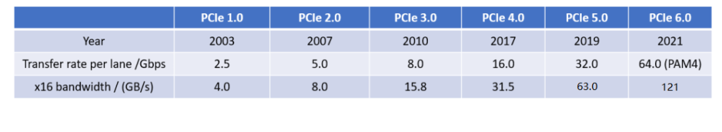
The parameters of each generation of PCIe are shown in the following table.
From the perspective of the rate of a single lane, NVLink is generally about twice as high as PCIe of the same period, and the advantage of total bandwidth is even more obvious, NVLink is about five times the total bandwidth of PCIe. It has been surpassing and never stopped.
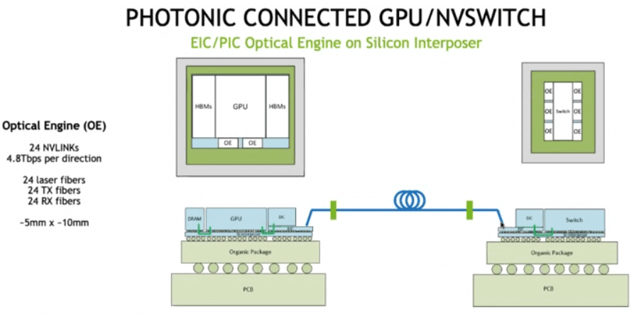
NVLink, after nearly a decade of development, has become a core technology in Nvidia GPU chips, an important part of its ecosystem, effectively solving the problem of high-bandwidth and low-latency data interconnection between GPU chips and changing the traditional computing architecture. However, since this technology is unique to Nvidia, other AI chip companies can only use PCIe or other interconnection protocols. At the same time, Nvidia is exploring the use of optical interconnection to achieve the connection between GPUs, as shown in the figure below, where the silicon photonics chip and the GPU are co-packaged together, and optical fibers connect two GPU chips.
Source: https://www.nextplatform.com/2022/08/17/nvidia-shows-what-optically-linked-gpu-systems-might-look-like/
Related Products:
-
 NVIDIA MMA4Z00-NS400 Compatible 400G OSFP SR4 Flat Top PAM4 850nm 30m on OM3/50m on OM4 MTP/MPO-12 Multimode FEC Optical Transceiver Module
$550.00
NVIDIA MMA4Z00-NS400 Compatible 400G OSFP SR4 Flat Top PAM4 850nm 30m on OM3/50m on OM4 MTP/MPO-12 Multimode FEC Optical Transceiver Module
$550.00
-
NVIDIA MMA4Z00-NS-FLT Compatible 800Gb/s Twin-port OSFP 2x400G SR8 PAM4 850nm 100m DOM Dual MPO-12 MMF Optical Transceiver Module
$650.00
-
NVIDIA MMA4Z00-NS Compatible 800Gb/s Twin-port OSFP 2x400G SR8 PAM4 850nm 100m DOM Dual MPO-12 MMF Optical Transceiver Module
$650.00
-
NVIDIA MMS4X00-NM Compatible 800Gb/s Twin-port OSFP 2x400G PAM4 1310nm 500m DOM Dual MTP/MPO-12 SMF Optical Transceiver Module
$900.00
-
NVIDIA MMS4X00-NM-FLT Compatible 800G Twin-port OSFP 2x400G Flat Top PAM4 1310nm 500m DOM Dual MTP/MPO-12 SMF Optical Transceiver Module
$1199.00
-
NVIDIA MMS4X00-NS400 Compatible 400G OSFP DR4 Flat Top PAM4 1310nm MTP/MPO-12 500m SMF FEC Optical Transceiver Module
$700.00
-
NVIDIA(Mellanox) MMA1T00-HS Compatible 200G Infiniband HDR QSFP56 SR4 850nm 100m MPO-12 APC OM3/OM4 FEC PAM4 Optical Transceiver Module
$139.00
-
NVIDIA MFP7E10-N010 Compatible 10m (33ft) 8 Fibers Low Insertion Loss Female to Female MPO Trunk Cable Polarity B APC to APC LSZH Multimode OM3 50/125
$47.00
-
NVIDIA MCP7Y00-N003-FLT Compatible 3m (10ft) 800G Twin-port OSFP to 2x400G Flat Top OSFP InfiniBand NDR Breakout DAC
$260.00
-
NVIDIA MCP7Y70-H002 Compatible 2m (7ft) 400G Twin-port 2x200G OSFP to 4x100G QSFP56 Passive Breakout Direct Attach Copper Cable
$155.00
-
NVIDIA MCA4J80-N003-FTF Compatible 3m (10ft) 800G Twin-port 2x400G OSFP to 2x400G OSFP InfiniBand NDR Active Copper Cable, Flat top on one end and Finned top on other
$600.00
-
NVIDIA MCP7Y10-N002 Compatible 2m (7ft) 800G InfiniBand NDR Twin-port OSFP to 2x400G QSFP112 Breakout DAC
$190.00